Transmission structure of radio-frequency signal in semiconductor device and forming method for transmission structure

A technology of radio frequency signal and transmission structure, applied in the fields of semiconductor devices, semiconductor/solid-state device manufacturing, semiconductor/solid-state device components, etc., can solve the problems of low signal linearity, complex RF signal formation methods, and poor signal quality, To achieve the effect of saving process time

Active Publication Date: 2012-04-25
SHANGHAI HUAHONG GRACE SEMICON MFG CORP
View PDF6 Cites 0 Cited by
  • Summary
  • Abstract
  • Description
  • Claims
  • Application Information

AI Technical Summary

Problems solved by technology

[0009] However, the formation method of the transmission structure of the radio frequency signal in the semiconductor device formed in the prior art is complicated, and the transmission structure of the radi

Method used


Image

  • Transmission structure of radio-frequency signal in semiconductor device and forming method for transmission structure
  • Transmission structure of radio-frequency signal in semiconductor device and forming method for transmission structure
  • Transmission structure of radio-frequency signal in semiconductor device and forming method for transmission structure

Examples


Example Embodiment

[0033] As described in the background, the method for forming the transmission structure of the radio frequency signal in the semiconductor device in the prior art is complex, and the formed transmission structure of the radio frequency signal in the semiconductor device has poor linearity of the radio frequency signal received by the receiving end.

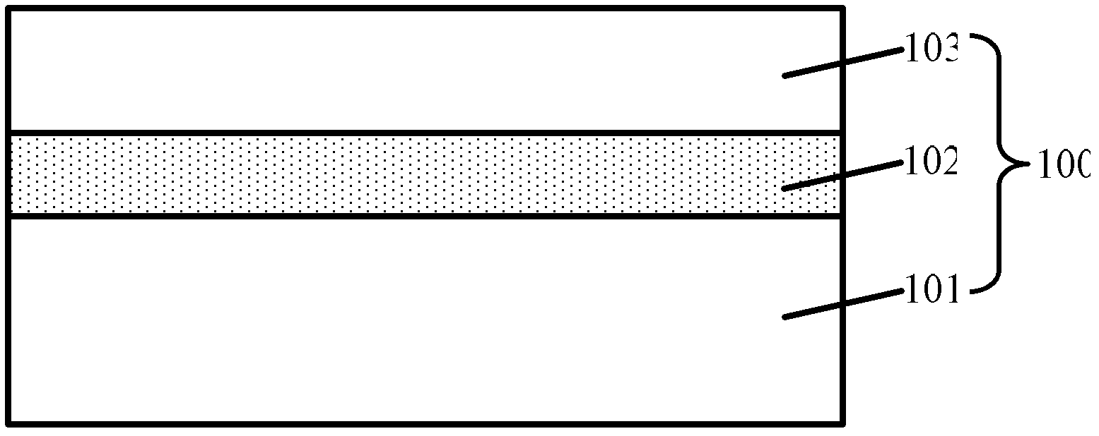
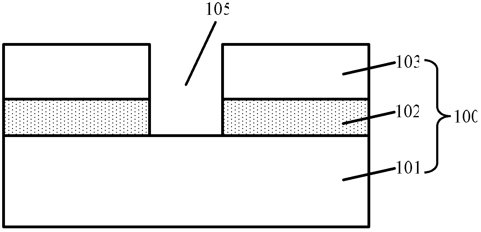
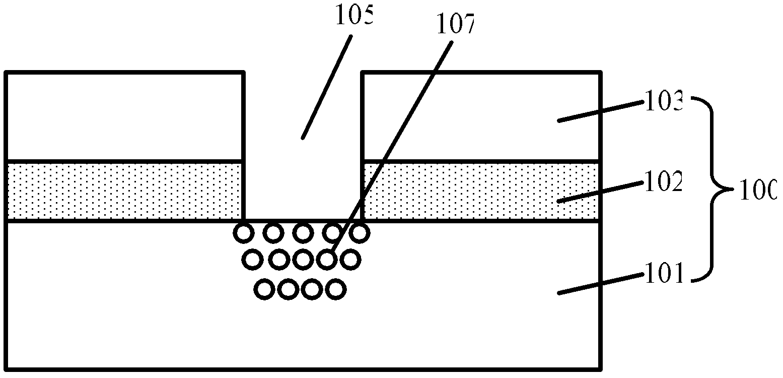
[0034] After research, the inventor of the embodiment of the present invention found that please continue to refer to Figure 5 , the prior art uses a silicon-on-insulator substrate as a shielding layer, but since the back substrate 101, the oxide layer 102 and the silicon film 103 in the silicon-on-insulator substrate 100 form a capacitance (not marked), the capacitance will reflect A part of the radio frequency signal, the reflected part of the signal will be absorbed by the metal layer 113 again; and because the capacitance has different reflection degrees for signals of different frequencies, the linear relationship of the rad...


PUM


Abstract

The embodiment of the invention provides a forming method for a transmission structure of a radio-frequency signal in a semiconductor device. The forming method comprises the following steps of: providing a silicon substrate on an insulator; forming a conducting layer on the surface of the silicon substrate, which is positioned on part of the insulator, wherein the conducting layer is grounded; and forming an interconnected metal layer covering the silicon substrate on the insulator and the conducting layer, wherein the interconnected metal layer comprises a dielectric layer and a metal layer positioned in the dielectric layer and the metal layer is positioned above the conducting layer. The forming method in the embodiment of the invention has a simple process. Correspondingly, the embodiment of the invention also provides the transmission structure of the radio-frequency signal in the semiconductor device. The radio-frequency signal is transmitted by the transmission structure; and the radio-frequency signal received by a receiving end has favorable linearity and high quality.

Description

technical field [0001] The invention relates to the technical field of semiconductors, in particular to a transmission structure of a radio frequency signal in a semiconductor device and a forming method thereof. Background technique [0002] As semiconductor technology develops, it is often desirable to include more functions on a single integrated circuit in order to reduce manufacturing and design costs. For example, in wireless communication systems, it may be desirable to include radio frequency circuitry on the same integrated circuit as digital logic circuitry. [0003] In the prior art, if an ordinary substrate is directly used to form an integrated circuit including both digital logic circuits and radio frequency circuits, the radio frequency circuit will cause coupling between the substrate and the integrated circuit inductor, and the inductance performance of the integrated circuit inductor decline. In order to integrate more functions on a single integrated cir...

Claims


Application Information

Patent Timeline
IPC IPC(8): H01L21/02H01L23/552
Inventor 刘巍李乐孔蔚然
Owner SHANGHAI HUAHONG GRACE SEMICON MFG CORP
Why Eureka
Try Eureka