Group III nitride enhancement mode HEMT (High Electron Mobility Transistor) device

A nitride, enhanced technology, used in semiconductor devices, electrical components, circuits, etc., can solve problems such as unsatisfactory effects

Inactive Publication Date: 2012-04-25
SUZHOU INST OF NANO TECH & NANO BIONICS CHINESE ACEDEMY OF SCI
View PDF2 Cites 8 Cited by
  • Summary
  • Abstract
  • Description
  • Claims
  • Application Information

AI Technical Summary

Problems solved by technology

However, the above method of suppressing current collapse is not ideal in the case of high current and high voltage.

Method used


Image

  • Group III nitride enhancement mode HEMT (High Electron Mobility Transistor) device
  • Group III nitride enhancement mode HEMT (High Electron Mobility Transistor) device
  • Group III nitride enhancement mode HEMT (High Electron Mobility Transistor) device

Examples


Embodiment approach

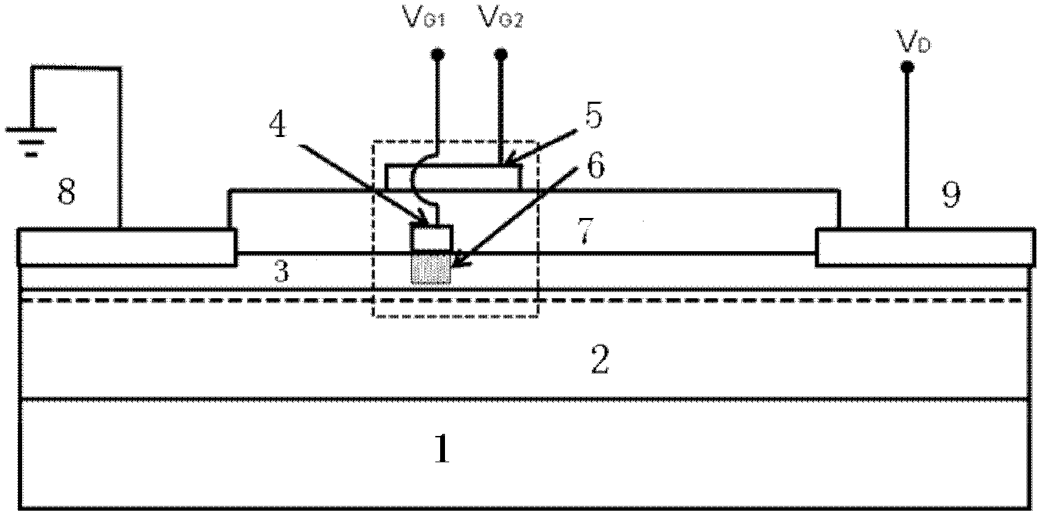
[0026] refer to image 3 , as a preferred embodiment of the present invention, the E-MODE HEMT has: a first semiconductor 13 (GaN), and a second semiconductor 14 (AlGaN) formed on the first semiconductor 13 . The first semiconductor 13 is not intentionally doped. The n-type impurity may or may not be doped in the second semiconductor 14 . The band gap of the second semiconductor 14 is wider than that of the first semiconductor 13 . The thickness of the second semiconductor 14 is about 15 to 30 nm. The first semiconductor 13 and the second semiconductor 14 form a heterostructure, forming a two-dimensional electron gas (2DEG) at the interface.

[0027] This E-MODE HEMT has a drain electrode 11 and a source electrode 12 arranged at a predetermined distance apart. The drain electrode 11 and the source electrode 12 extend through the second semiconductor 14 to the first semiconductor 13 and are connected to the two-dimensional electron gas in the channel. The drain electrode 1...


PUM


Abstract

The invention discloses a group III nitride enhancement mode HEMT (High Electron Mobility Transistor) device which comprises source and drain electrodes, main and accessory grids, an insulating medium layer and a heterostructure, wherein the source and drain electrodes are electrically connected by two-dimensional electron formed in the heterostructure; the heterostructure comprises a first semiconductor and a second semiconductor; the first semiconductor is arranged between the source and drain electrodes; the second semiconductor is formed on the surface of the first semiconductor and is provided with a band gap which is wider than the first semiconductor; the main grid is arranged at one side of the surface of the second semiconductor near the source electrode and forms schottky contact with the second semiconductor, and a plasma processing area is also formed in the local area of the second semiconductor under the main grid; a medium layer is formed on the surfaces of the second semiconductor and the main grid and between the source and drain electrodes; and the accessory grid is formed on the surface of the medium layer, the edge of at least one side of the accessory grid extends to the direction of the source electrode or drain electrode, and the orthographic projection of the accessory grid is laminated with the edges of both sides of the main grid. The group III nitride enhancement mode HEMT device can effectively inhibit the current collapse effect fundamentally.

Description

technical field [0001] The invention relates to an enhancement-mode high electron mobility transistor (Enhancement-mode High Electron Mobility Transistor, E-mode HEMT), in particular to a Group III nitride enhanced HEMT device. Background technique [0002] When the HEMT device uses group III nitride semiconductors, due to the piezoelectric polarization and spontaneous polarization effects, a high-concentration two-dimensional electron gas can be formed on the heterostructure (Heterostructure), such as AlGaN / GaN. In addition, HEMT devices use group III nitride semiconductors, which can obtain high insulation breakdown electric field strength and good high temperature resistance characteristics. HEMTs with group III nitride semiconductors with heterostructures can be used not only as high-frequency devices, but also as high-voltage, high-current power switching devices. When applied to high-power switching circuits, for the sake of simple circuit design and safety considerat...

Claims


Application Information

Patent Timeline
Patent Type & Authority Applications(China)
IPC IPC(8): H01L29/778H01L29/423
Inventor 蔡勇于国浩董志华王越张宝顺
Owner SUZHOU INST OF NANO TECH & NANO BIONICS CHINESE ACEDEMY OF SCI
Why Eureka
Try Eureka