Method for effectively reducing water mark defects
A technology for water marks and defects, applied in the field of etching of semiconductor wafers, can solve the problems of different hydrophobicity and water marks, etc.
- Summary
- Abstract
- Description
- Claims
- Application Information
AI Technical Summary
Problems solved by technology
Method used
Image
Examples
Embodiment Construction
[0028] The present invention will be described in further detail below in conjunction with the accompanying drawings and specific embodiments. The specific embodiments described here are only used to explain the present invention, and are not used to limit the protection scope of the present invention.
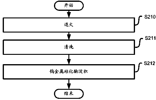
[0029] Before adopting the method of the present invention, first process the wafer according to the prior art Dual Poly Gate (double polysilicon gate) process, and after performing the step of wafer annealing, use the method of the present invention to perform the cleaning process, and the cleaning process includes the following steps :
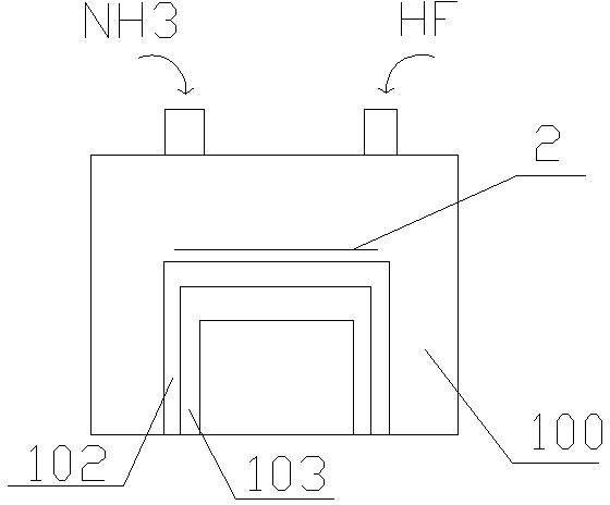
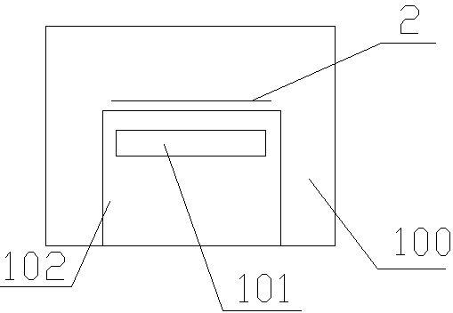
[0030] The wafer is sent into a wet etching cleaning system to perform a subsequent wet etching process on the wafer; then the wafer is wet etched to remove organic matter and particles, and then the wafer is dried to make the wafer The surface of the wafer is a hydrophilic surface to reduce the formation of water mark defects; and then dry...
PUM
 Abstract
Description
Claims
Application Information
 - R&D Engineer
- R&D Manager
- IP Professional
- Industry Leading Data Capabilities
- Powerful AI technology
- Patent DNA Extraction
Browse by: Latest US Patents, China's latest patents, Technical Efficacy Thesaurus, Application Domain, Technology Topic, Popular Technical Reports.
© 2024 PatSnap. All rights reserved.Legal|Privacy policy|Modern Slavery Act Transparency Statement|Sitemap|About US| Contact US: help@patsnap.com


