Heterojunction with intrinsic thin layer (HIT) solar cell structure with heterogeneous floating junction back passivation, and preparation process thereof

A solar cell and preparation process technology, applied in the field of solar cells, can solve the problems such as the attenuation of amorphous silicon cell efficiency, the increase of photo-generated carrier recombination, the reduction of quantum efficiency of amorphous silicon thin film cells, etc., and achieves low surface recombination rate, Good open circuit voltage, improving the effect of open circuit voltage and overall efficiency

Active Publication Date: 2013-11-20
TRINA SOLAR CO LTD
View PDF3 Cites 0 Cited by
  • Summary
  • Abstract
  • Description
  • Claims
  • Application Information

AI Technical Summary

Problems solved by technology

[0003] There is a problem of attenuation of efficiency in amorphous silicon solar cells based entirely on thin-film technology. The reason is that the light-absorbing layer of amorphous silicon thin-film solar cells is an amorphous silicon layer with a thickness of several hundred nanometers. It will produce a photogenerated metastable state, which will increase the recombination of photogenerated carriers and reduce the quantum efficiency of amorphous silicon thin film cells, that is, the S-W effect.

Method used


Image

  • Heterojunction with intrinsic thin layer (HIT) solar cell structure with heterogeneous floating junction back passivation, and preparation process thereof
  • Heterojunction with intrinsic thin layer (HIT) solar cell structure with heterogeneous floating junction back passivation, and preparation process thereof
  • Heterojunction with intrinsic thin layer (HIT) solar cell structure with heterogeneous floating junction back passivation, and preparation process thereof

Examples


Embodiment Construction

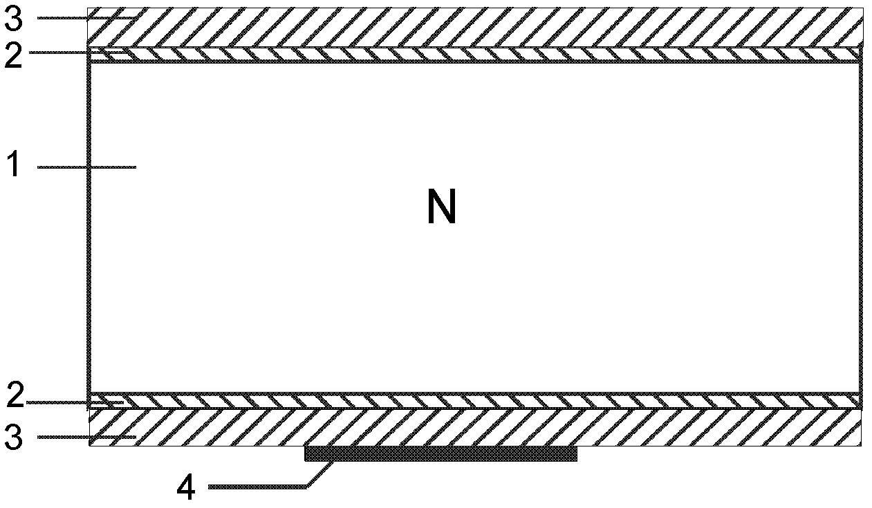
[0041] The HIT solar cell structure and preparation process of the heterogeneous floating junction back passivation, the basic idea is to deposit a P-type amorphous silicon layer 3 on the upper surface and the lower surface of the N-type crystalline silicon substrate 1 to form a heterogeneous P-N junction Structure, the floating of the P-N junction on the back of the N-type crystalline silicon substrate 1 is realized by vapor deposition of the insulating film layer 5, while the back electrode is still realized by N-type amorphous silicon deposition. The N-type amorphous silicon back electrode and the P-type amorphous silicon floating junction back passivation structure are strictly separated by the insulating film layer 5, which ensures a good floating junction back passivation effect.

[0042] First, unlike Sanyo's HIT battery process, this process deposits an amorphous silicon P-N heterostructure layer on the upper and lower surfaces of the N-type crystalline silicon substrat...


PUM


Abstract

The invention relates to the technical field of solar cells, in particular to a heterojunction with intrinsic thin layer (HIT) solar cell structure with heterogeneous floating junction back passivation, and a preparation process thereof. P-type amorphous silicon layers are deposited on the upper surface and the lower surface of an N-type crystal silicon substrate so as to form heterogeneous P-N junction structures; a mask is manufactured on the heterogeneous P-N junction structure on the lower surface; selective etching is performed so as to form isolated heterogeneous P-N junction structures; the mask layer is removed and an insulation thin film layer is deposited on the lower surface; a mask is manufactured on the insulation thin film layer; secondary selective etching is performed, so that the side surface and the back surface of the heterogeneous P-N junction structure on the lower surface of the N-type crystal silicon substrate are encircled by the insulation thin film layer, and a floating junction back passivation structure is formed; and an N-type amorphous silicon back electrode and a P-type amorphous silicon floating junction back passivation structure are strictly separated from each other by the insulation thin film layer. Compared with an HIT standard process and a structure of the Sanyo, the HIT solar cell structure has the advantages that: the floating P-N junction back passivation structure is introduced into the back surface of the N-type crystal silicon, so that the surface compounding rate is lower and the open-circuit voltage is higher.

Description

technical field [0001] The invention relates to the technical field of solar cells, in particular to a HIT solar cell structure with heterogeneous floating junction back passivation and a preparation process thereof. Background technique [0002] Solar power generation is currently the most potential green and clean energy, and high-efficiency solar cells are the core of solar power generation. At present, the battery material with the highest industrialization and maturity of solar cells is still crystalline silicon cells, but the solar cell technology that will achieve parity in the grid in the future should be solar cells based on thin-film technology. Among the existing high-efficiency crystalline silicon cell technologies, the rear passivation technology has the greatest difference. The degree of back passivation of crystalline silicon not only affects the long-wave incident light response and open circuit voltage of solar cells, but also affects the temperature charac...

Claims


Application Information

Patent Timeline
Patent Type & Authority Patents(China)
IPC IPC(8): H01L31/18H01L31/0352H01L31/078H01L31/0224
CPCH01L31/0747H01L31/022425Y02E10/50
Inventor 王旺平
Owner TRINA SOLAR CO LTD
Why Eureka
Try Eureka