
Optical modeling proximity correction method of SRAM (Static Random Access Memory) grid dimension

A technology of proximity correction and gate size, which is applied in the direction of optics, photolithography on the pattern surface, and originals for photomechanical processing, etc., can solve the problems of reducing the process window of lithography and device performance, and achieve large process window effect

Inactive Publication Date: 2012-05-09
SHANGHAI HUALI MICROELECTRONICS CORP
View PDF5 Cites 4 Cited by
  • Summary
  • Abstract
  • Description
  • Claims
  • Application Information

AI Technical Summary

Problems solved by technology

In the actual process, for different SRAM gate structures, there are different substrates, and correspondingly there will be slight correction errors caused by inaccurate models.
In today's advanced lithography process, the process window of lithography and the performance of the device will be reduced due to the subtle difference of optical effects

Method used


Image

  • Optical modeling proximity correction method of SRAM (Static Random Access Memory) grid dimension
  • Optical modeling proximity correction method of SRAM (Static Random Access Memory) grid dimension
  • Optical modeling proximity correction method of SRAM (Static Random Access Memory) grid dimension

Examples


Embodiment Construction

[0017] The specific embodiment of the present invention will be further described below in conjunction with accompanying drawing:

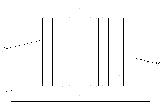
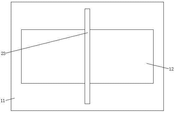
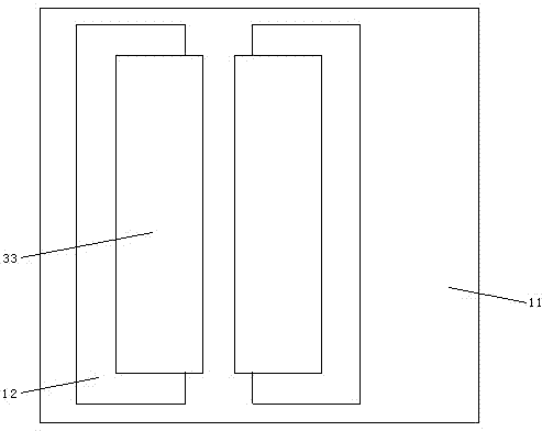
[0018] Such as Figure 1-5 As shown, the optical modeling approach correction method of the SRAM gate size of the present invention, first, prepare a test wafer, and design the line width size, spacing size, pitch, line end spacing size and active area according to the process requirements Design the pattern of the active area mask and the gate mask in terms of size, etc.; secondly, on the test wafer, use the active area mask to carry out the active area preparation process on the test wafer to form the active area 12; after that , continue the shallow trench process, after forming the shallow trench isolation region 11 surrounding the active region 12, the gate process is performed, and the gate mask is used to form the dense line size test structure design on the active region respectively during the photolithography process Domain 13 (as figu...


PUM


Abstract

The invention relates to the semiconductor manufacturing field, in particular to an optical modeling proximity correction method of SRAM (Static Random Access Memory) grid dimension. The invention discloses an optical modeling proximity correction method of SRAM grid dimension, comprising a step of establishing an optical grid proximity effect model with substrate information through test reticle mask design and model data acquisition, thereby achieving the purpose of predicting spacing distances among grid line terminals precisly and ensuring a craft window big enough for a photoetching process of the grid.

Description

technical field [0001] The invention relates to the field of semiconductor manufacturing, in particular to an optical modeling proximity correction method for SRAM gate size. Background technique [0002] In the manufacturing process of semiconductor devices, with the rapid development of ultra-large-scale integrated circuits, while the integration of chips is getting higher and higher, the chip size is getting smaller and smaller. In the lithography process, the exposure pattern is also getting smaller, especially after entering the 65nm process, the control requirements for the gate size are more stringent, and higher requirements are put forward for the lithography process and optical proximity correction. The subtle differences in optical effects have already affected the process window of lithography and the performance of devices. [0003] In today's advanced photolithography process, due to the reduction in the size of the exposure pattern, the optical proximity corr...

Claims


Application Information

Patent Timeline
IPC IPC(8): G03F1/36H01L21/28
Inventor 魏芳张辰明
Owner SHANGHAI HUALI MICROELECTRONICS CORP
Learn More