Silicon-on-insulator laterally diffused metal oxide semiconductor (SOI LDMOS) device containing composite drift region

A drift region and device technology, applied in the direction of semiconductor devices, electrical components, circuits, etc., can solve the problem of increasing the on-state voltage drop

Inactive Publication Date: 2012-05-09
PEKING UNIV
View PDF2 Cites 8 Cited by
  • Summary
  • Abstract
  • Description
  • Claims
  • Application Information

AI Technical Summary

Problems solved by technology

However, the current SOI LDMOS devices have the following defects: if the brea

Method used


Image

  • Silicon-on-insulator laterally diffused metal oxide semiconductor (SOI LDMOS) device containing composite drift region
  • Silicon-on-insulator laterally diffused metal oxide semiconductor (SOI LDMOS) device containing composite drift region
  • Silicon-on-insulator laterally diffused metal oxide semiconductor (SOI LDMOS) device containing composite drift region

Examples


Embodiment Construction

[0019] In order to make the purpose, content, and advantages of the present invention clearer, the implementation manners of the present invention will be further described in detail below in conjunction with the accompanying drawings.

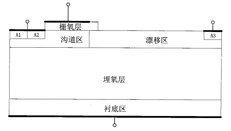
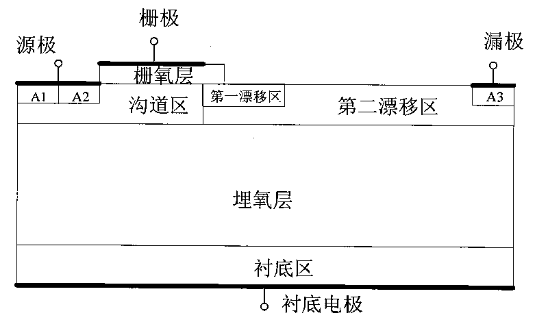
[0020] Such as figure 2 As shown, the SOI LDMOS device containing the composite drift region according to the embodiment of the present invention sequentially includes a gate oxide layer, a top silicon layer, a buried oxide layer and a bottom silicon layer (ie figure 2 The substrate region in), wherein the top layer silicon includes a channel region and a composite drift region, and the composite drift region includes a first drift region and a second drift region, wherein the thickness of the first drift region is smaller than the thickness of the top layer silicon .

[0021] The channel region is a P channel region (that is, a P-type doped channel region), and correspondingly, the second drift region is an N-type drift region (that is, an...


PUM


Abstract

The invention discloses a silicon-on-insulator laterally diffused metal oxide semiconductor (SOI LDMOS) device containing a composite drift region. The device sequentially comprises a grid oxide layer, a top silicon layer, a buried oxide layer and a bottom silicon layer from top to bottom, wherein the top silicon layer contains the composite drift region; and the composite drift region contains a first drift region and a second drift region, wherein the first drift region is adjacent to a channel region and is encircled by the second drift region. By adopting the composite drift region in the device, the maximum electric field value of the drift region close to one end of the channel, and the breakdown voltage value is improved; and because the first drift region is thinner than the top silicon layer, the additional value of the on resistance caused by the first drift region is reduced, and the on conduction property is improved.

Description

technical field [0001] The invention relates to the field of high-voltage semiconductor devices, in particular to an SOI LDMOS device containing a composite drift region. Background technique [0002] LDMOS (Laterally Diffused Metal Oxide Semiconductor) process technology is a high-voltage semiconductor device widely used in radio frequency base stations, PDP (Plasma Display Panel, plasma display) display drivers, and automotive electronics. Compared with the traditional IGBT (Insulated Gate Bipolar Transistor, insulated gate bipolar transistor), it has higher response speed and lower leakage current, and as a planar device, it is more conducive to process integration, but it also brings open state increase in resistance. [0003] The combination of SOI (Silicon-On-Insulator, silicon on insulator) technology and LDMOS greatly improves the isolation characteristics of the device, greatly reduces the mutual interference between the low-voltage control circuit and the high-vol...

Claims


Application Information

Patent Timeline
IPC IPC(8): H01L29/78H01L29/06
Inventor 竺明达杜刚刘晓彦
Owner PEKING UNIV
Why Eureka
Try Eureka