Semiconductor module

A semiconductor and chip technology, applied in the direction of semiconductor devices, semiconductor/solid-state device components, electric solid-state devices, etc., can solve the problems of position shift, difficulty in manufacturing semiconductor modules with high yield, and difficulty in high precision, etc. The effect of yield

Inactive Publication Date: 2012-05-16
SANKEN ELECTRIC CO LTD
View PDF6 Cites 0 Cited by
  • Summary
  • Abstract
  • Description
  • Claims
  • Application Information

AI Technical Summary

Problems solved by technology

When the number of semiconductor chips to be mounted increases, it is difficult to maintain the accuracy of the above-mentioned positional relationship at a high level.
In particular, when the solder used for bonding is melted, semiconductor chips and leads move, so their positions shift
[0011] Therefore, it is difficult to manufacture a semiconductor module mounting a plurality of semiconductor chips with a high yield.

Method used


Image

  • Semiconductor module
  • Semiconductor module
  • Semiconductor module

Examples


Embodiment Construction

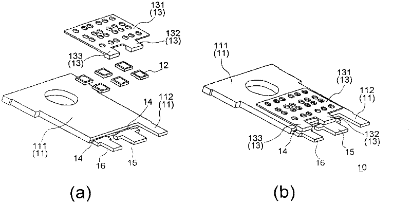
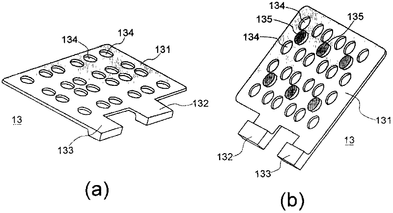
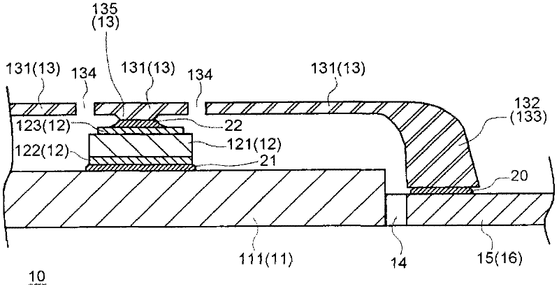
[0045] Hereinafter, the semiconductor module and its manufacturing method according to the embodiment of the present invention will be described. In this semiconductor module, a plurality of semiconductor chips are joined by soldering and mounted on the same lead frame. The mounted semiconductor chips have the same specifications and each has two electrodes (anode electrode, cathode electrode). Among them, one electrode of all the semiconductor chips is connected to the lead frame by solder. The other electrodes of all the semiconductor chips are connected to clip leads provided to cover the upper portions of all the semiconductor chips. With this structure, all the semiconductor chips are connected in parallel, the lead frame side is an electrode of one pole, and the clip lead side is an electrode of the other pole.

[0046] figure 1 It is an exploded perspective view ((a)) and an assembled perspective view ((b)) showing the structure of the semiconductor module 10 . In t...


PUM


Abstract

The present invention provides a semiconductor module. The semiconductor module which carries a plurality of semiconductor chips is machined through a high yield rate. In the semiconductor module (10), six semiconductor chips (12) are layed on a lead frame (11) through a 2*3 layout, and furthermore a clip type lead (13) is equipped whereon. Electric connection between the semiconductor module (10) and outside is performed through the following components: a first lead (112) which is used as one part of the lead frame (11), a second lead (15) and a third lead (16) which are separated through an insulation part (14) and are fixed on the lead frame (11). A clip lead body (131) is provided with 24 circular openings. The back side of the clip type lead body (131) is provided with six projections. The six projections are formed correspondingly to six semiconductor chips (12) and are jointed with the semiconductor chips (12) through a soldering layer.

Description

technical field [0001] The present invention relates to a structure of a semiconductor module which mounts a plurality of semiconductor chips and connects these semiconductor chips in parallel. Background technique [0002] In a power semiconductor module that operates with a large current, a structure in which a plurality of semiconductor chips are mounted on the same lead frame is often used. In this case, by simultaneously mounting different types of semiconductor chips, the power semiconductor module can be multifunctionalized. [0003] The form of the semiconductor module in this case is described in Patent Document 1, for example. In this technology, an IGBT (Insulated Gate Bipolar Transistor: Insulated Gate Bipolar Transistor) chip and a freewheeling diode chip are mounted on a single lead frame. The lead frame is used as wiring for connecting these chips, and leads formed into curved shapes by processing a flat plate are connected to the upper sides of these chips ...

Claims


Application Information

Patent Timeline
Patent Type & Authority Applications(China)
IPC IPC(8): H01L23/49H01L23/495
CPCH01L2224/32245H01L2924/13055H01L2924/12032H01L2924/1305H01L2224/40245H01L24/40H01L2224/37011H01L2924/00014H01L2224/84801H01L2224/37H01L2224/40H01L2224/83801H01L24/84H01L2924/00H01L2224/37099
Inventor 荻野博之上野成则
Owner SANKEN ELECTRIC CO LTD
Why Eureka
Try Eureka