Method for forming semiconductor device

A semiconductor and device technology, applied in the field of semiconductor device formation, can solve the problems of high price of platinum metal, increase the difficulty of etching nickel alloy layer, and increase the cost of process manufacturing, so as to strengthen the diffusion barrier, improve the leakage performance of devices, reduce generated effect

Active Publication Date: 2013-12-04
SEMICON MFG INT (SHANGHAI) CORP +1
View PDF1 Cites 0 Cited by
  • Summary
  • Abstract
  • Description
  • Claims
  • Application Information

AI Technical Summary

Problems solved by technology

However, the higher price of platinum metal leads to an increase in the manufacturing cost of the process; at the same time, a higher content of platinum will increase the etching difficulty of removing the excess nickel alloy layer

Method used


Image

  • Method for forming semiconductor device
  • Method for forming semiconductor device
  • Method for forming semiconductor device

Examples


Embodiment Construction

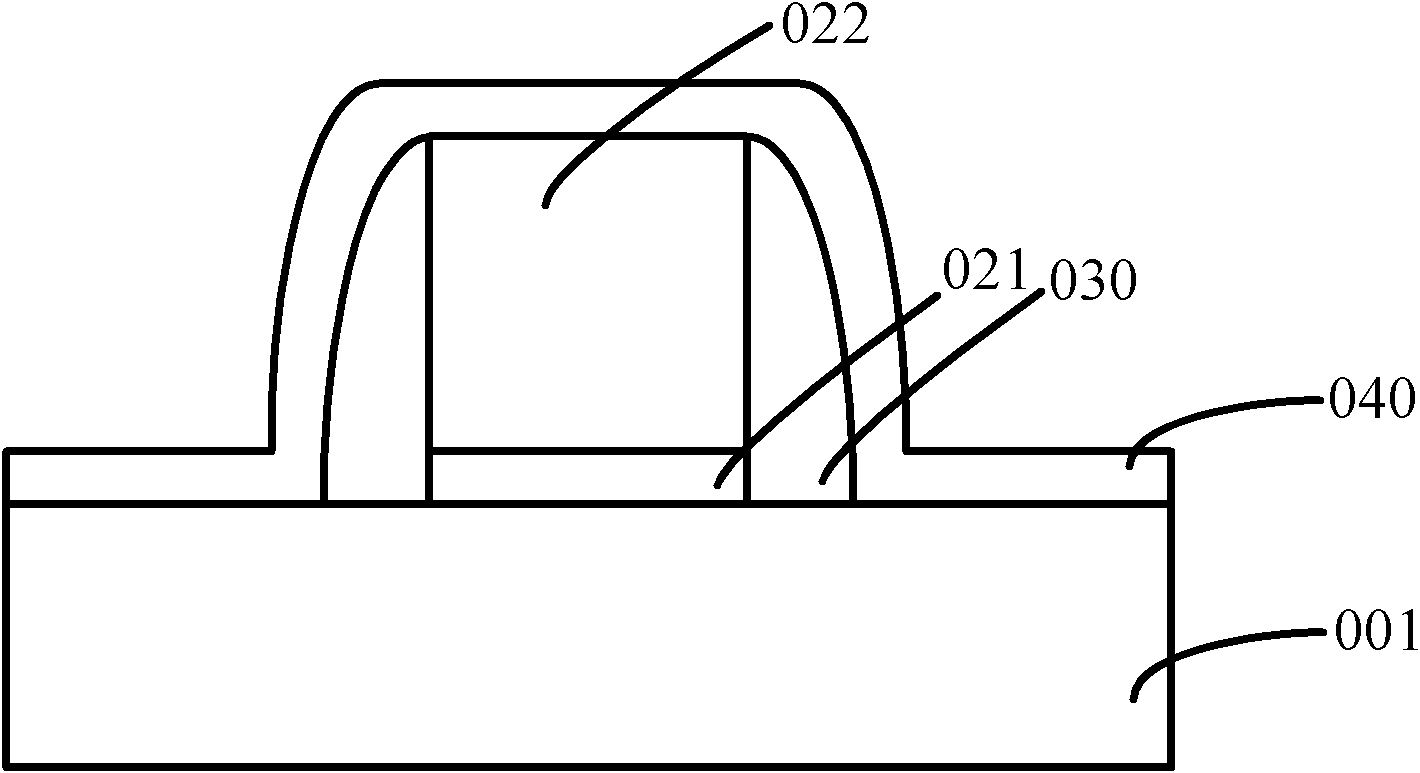
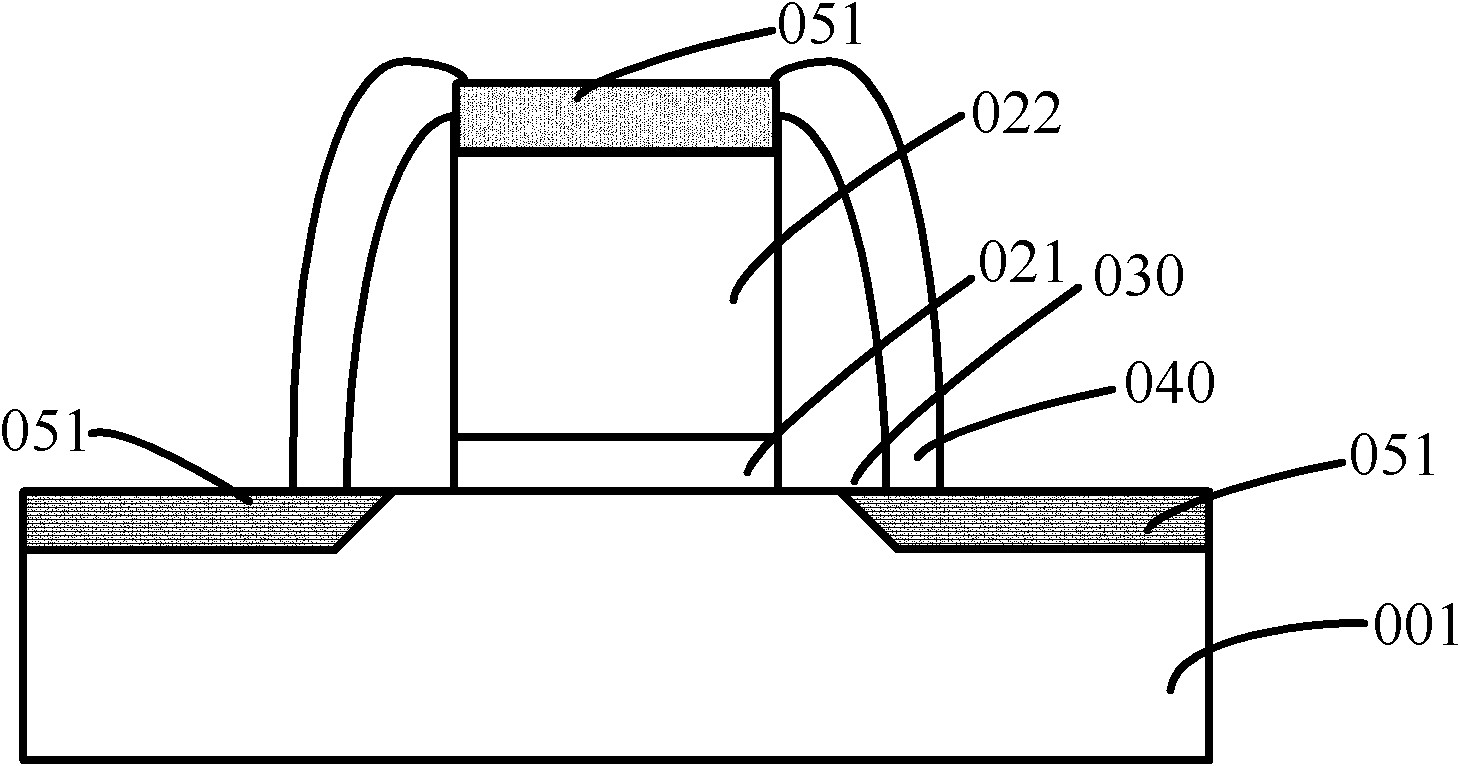
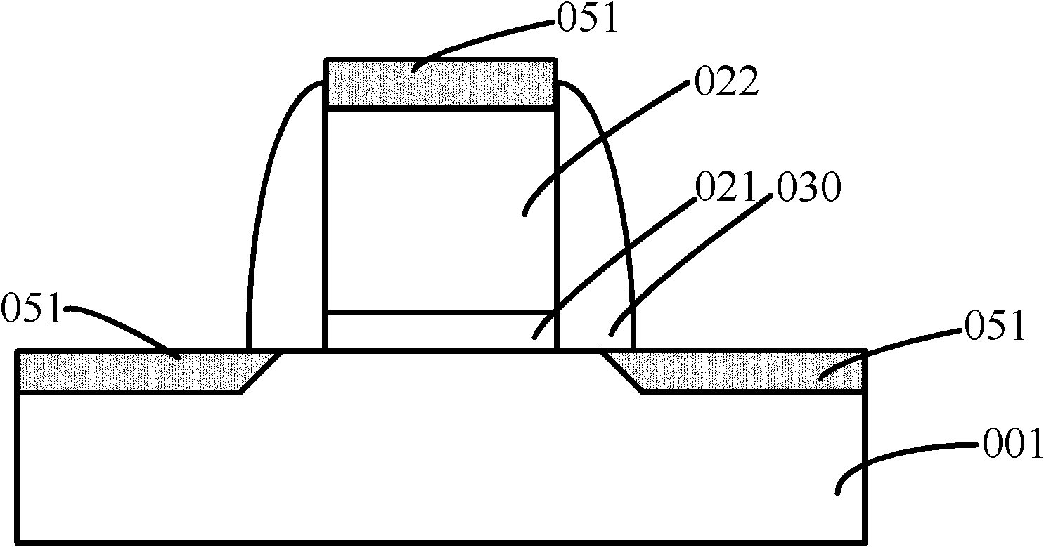
[0029] In the prior art nickel silicide technology, NiSi formed by nickel diffusion 2 The layer will worsen the channel leakage, and increasing the platinum content will cause the cost to rise. Based on the above problems, the inventor conducted a series of experiments, mainly by changing the thickness of the nickel alloy layer, to compare and study the concentration relationship of each metal in the nickel silicide generated by the nickel alloy layer in the substrate. In this experiment, the nickel alloy layer is an alloy layer of nickel and platinum.

[0030] Such as Figure 5 As shown, it is a schematic diagram of the concentration distribution of nickel in the nickel silicide layer in the substrate. The abscissa represents the depth of the substrate, and the ordinate represents the concentration of nickel contained in the position corresponding to the depth of the substrate. Such as Image 6 As shown, it is a schematic diagram of the concentration distribution of platinum in ...


PUM

PropertyMeasurementUnit
thicknessaaaaaaaaaa
thicknessaaaaaaaaaa
thicknessaaaaaaaaaa

Abstract

The invention provides a method for forming a semiconductor device, comprising the following steps: providing a substrate, a grid structure positioned on the substrate and a source area and a drain area which are both positioned in two side substrates of the grid structure; forming a nickel alloy layer on the exposed substrate surface containing nickel and at least one of other metals and having the thickness of 150-400 angstrom; and annealing the nickel alloy layer to form a nickel silicide in the substrate. According to the method, the diffusing capacity of the subsequently-formed nickel silicide in platinum is improved through improving the thickness of the nickel alloy layer which is in the range of 150-400 angstrom to enhance the diffusion barrier performance of the platinum element to the nickel element, thereby avoiding the diffusion of nickel to channel regions below a gate oxidation layer, reducing the generation of NiSi2 layers and improving the problem of deteriorating the electric leakage performance due to the development of the NiSi2 layer to channels.

Description

Technical field [0001] The present invention relates to the field of semiconductor manufacturing, and in particular to a method for forming semiconductor devices. Background technique [0002] The salicide technology is a process technology that reduces the resistance of the gate electrode and the source / drain region by forming a metal silicide layer on the gate electrode and the source / drain region. The nickel silicide layer and the cobalt silicide layer are widely used as the metal silicide layer. The Chinese patent application with the patent publication number CN101432860A provides a technical solution that uses a nickel silicide layer as a metal silicide. [0003] The nickel silicide layer formed by the nickel salicide technology can have different composition ratios. For example, the nickel silicide layer can be Ni 2 Si layer, NiSi layer or NiSi 2 Any of the layers. Among them, the composition of different silicides is determined by the ratio of nickel to silicon during th...

Claims


Application Information

Patent Timeline
Patent Type & Authority Patents(China)
IPC IPC(8): H01L21/28H01L21/283H01L21/336
Inventor 杨瑞鹏孔祥涛胡宇慧
Owner SEMICON MFG INT (SHANGHAI) CORP
Why Eureka
Try Eureka