Film for semiconductor and semiconductor device manufacturing method

A technology of semiconductor and supporting film, which is applied in semiconductor/solid-state device manufacturing, semiconductor device, transportation and packaging, etc. It can solve problems such as cracks and defects in semiconductor components, and achieve high manufacturing yield, high reliability, and anti-pickup properties Reduced effect

Inactive Publication Date: 2012-05-23
SUMITOMO BAKELITE CO LTD
View PDF6 Cites 6 Cited by
  • Summary
  • Abstract
  • Description
  • Claims
  • Application Information

AI Technical Summary

Problems solved by technology

Moreover, the above-mentioned problems will lead to defects such as cracks or defects in semiconductor elements when they are picked up.

Method used


Image

  • Film for semiconductor and semiconductor device manufacturing method
  • Film for semiconductor and semiconductor device manufacturing method
  • Film for semiconductor and semiconductor device manufacturing method

Examples


Embodiment approach

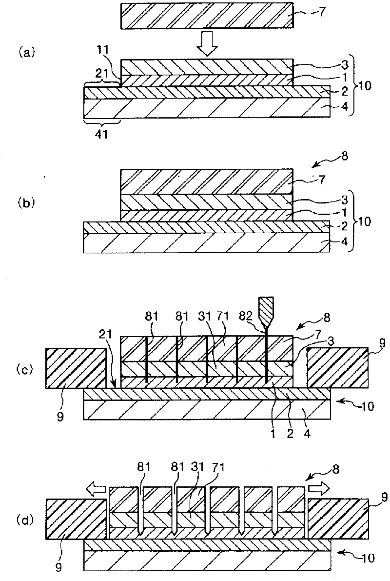
[0050] Figure 1 to Figure 3 It is a figure (longitudinal cross-sectional view) for explaining the first embodiment of the film for semiconductor of the present invention and the manufacturing method of the semiconductor device of the present invention; Figure 4 It is a figure for demonstrating the manufacturing method of the film for semiconductors of this invention. Additionally, in the description below, the Figure 1 to Figure 4 The upper side is called "upper" and the lower side is called "lower".

[0051] [Film for semiconductor]

[0052] figure 1 The film 10 for a semiconductor shown in has a support film 4 , a first adhesive layer 1 , a second adhesive layer 2 , and an adhesive layer 3 . More specifically, the film 10 for a semiconductor is formed by sequentially laminating the second adhesive layer 2 , the first adhesive layer 1 , and the adhesive layer 3 on the support film 4 .

[0053] Such as figure 1 As shown in (a), the above-mentioned semiconductor film...

no. 2 approach

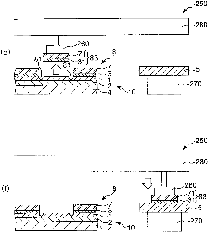
[0224] Next, a second embodiment of the film for a semiconductor of the present invention and the method of manufacturing a semiconductor device of the present invention will be described.

[0225] Figure 5 It is a figure (longitudinal sectional view) for demonstrating the 2nd Embodiment of the film for semiconductors of this invention, and the manufacturing method of the semiconductor device of this invention. Additionally, in the description below, the Figure 5 The upper side is called "upper" and the lower side is called "lower".

[0226] The second embodiment will be described below, but the description will focus on the parts different from the first embodiment, and the description of the same matters will be omitted. In addition, in Figure 5 In the same configuration as the first embodiment, the above-mentioned figure 1 The same notation as described in .

[0227] The semiconductor film 10 ′ in this embodiment is the same as that of the above-mentioned first emb...

Embodiment 1

[0247] Formation of the first adhesive layer

[0248] 100 parts by weight of a copolymer with a weight average molecular weight of 300,000 obtained by copolymerizing 30% by weight of 2-ethylhexyl acrylate and 70% by weight of vinyl acetate, 45 parts by weight of a pentafunctional acrylate monomer with a molecular weight of 700 , 5 parts by weight of 2,2-dimethoxy-2-phenylacetophenone and 3 parts by weight of toluene diisocyanate (CORONET T-100, Nippon Polyurethane Industry Co., Ltd. ) production) was applied to a polyester film having a thickness of 38 μm after peeling treatment so that the thickness after drying would be 10 μm, and then dried at 80° C. for 5 minutes. Then, the obtained coating film was irradiated with 500mJ / cm 2 Ultraviolet rays form a film of a first adhesive layer on a polyester film.

[0249] In addition, the Shore D hardness of the obtained first adhesive layer was 40.

[0250] Formation of the second adhesive layer

[0251] 100 parts by weight of a...


PUM

PropertyMeasurementUnit
softening pointaaaaaaaaaa
particle sizeaaaaaaaaaa
softening pointaaaaaaaaaa

Abstract

A film for semiconductor includes a support film, a second adhesive layer, a first adhesive layer and a bonding layer which are laminated together in this order. This film for semiconductor is configured so that it supports a semiconductor wafer laminated on the bonding layer thereof when the semiconductor wafer is diced and the bonding layer is selectively peeled off from the first adhesive layer when a chip is picked up. This film for semiconductor is characterized in that in the case where peel strength at 23 DEG C of the chip is defined as ''F 23 (cN / 25mm)'' and peel strength at 60 DEG C of the chip is defined as ''F 60 (cN / 25mm) '', F 23 is in the range of 10 to 80 and F 60 / F 23 is in the range of 0.3 to 5.5. This makes it possible to improve a pickup property of the chip, to thereby prevent generation of defects in a semiconductor element.

Description

technical field [0001] The present invention relates to a film for a semiconductor and a method for manufacturing a semiconductor device. Background technique [0002] In recent years, along with the high performance of electronic equipment and the expansion of applications in mobile devices, the demand for higher density and higher integration of semiconductor devices has been strengthened, and the increase in the capacity and density of IC packages has been progressing. [0003] In these semiconductor device manufacturing methods, first, an adhesive sheet is pasted on a semiconductor wafer made of silicon, gallium, arsenic, etc., and while the periphery of the semiconductor wafer is fixed with a wafer ring, the above-mentioned Semiconductor wafers are diced and separated (singulated) into individual semiconductor elements. Next, the following steps are performed: an unfolding step for separating the singulated individual semiconductor elements from each other, and a pick-...

Claims


Application Information

Patent Timeline
Patent Type & Authority Applications(China)
IPC IPC(8): H01L21/301C09J7/02C09J133/00C09J161/06C09J163/00H01L21/52C09J7/20
CPCC09J7/0296C09J2463/00C08F218/08C08F2220/1825H01L21/78H01L2924/15311C08L2203/206C08G18/7621C09J2203/326C09J2201/606C09J2201/61C08L63/00H01L2224/48091C09J2201/36C09J175/14H01L2224/32225H01L2224/92247C09J133/08H01L2224/83191H01L24/27H01L2224/48227H01L24/83C08L61/04H01L24/29C09J163/00H01L2924/10253C09J7/02H01L2224/73265C09J2433/00C08G18/6225H01L2924/15787H01L2924/181C09J7/20C08L2666/14Y10T428/2848Y10T428/24942Y10T428/24983C08F220/1804C09J2301/208C09J2301/304C09J2301/302H01L2924/00H01L2924/00014H01L2924/00012C08F220/1808C08F222/105C09J7/22C09J7/40C09J7/30C09J7/38C09J161/06
Inventor 安田浩幸平野孝
Owner SUMITOMO BAKELITE CO LTD
Why Eureka
Try Eureka