Film for semiconductor and semiconductor device manufacturing method
Inactive Publication Date: 2012-05-10
SUMITOMO BAKELITE CO LTD
View PDF5 Cites 4 Cited by
Summary
Abstract
Description
Claims
Application Information
AI Technical Summary
This helps you quickly interpret patents by identifying the three key elements:
Problems solved by technology
Method used
Benefits of technology
Benefits of technology
[0020]It is an object of the present invention to provide a film for semiconductor which can improve a pickup property and manufacture a semiconductor device having high reliability while preventing generation of defects in a semiconductor element, and a method for manufacturing a semiconductor device using such a film for semiconductor.
[0023]According to such a present invention, the film for semiconductor is configured so that a ratio of peel strength at a high temperature (60° C.) between the adhesive layer and the bonding layer to peel strength at a low temperature (23° C.) between the adhesive layer and the bonding layer becomes a predetermined value. Therefore, even in the case where heat is transferred to the chip when being picked up, it is possible to prevent a pickup property of the chip from being lowered. Therefore, according to the present invention, it is possible to obtain a film for semiconductor which can improve a yield ratio of manufacturing semiconductor devices and to manufacture semiconductor devices each having high reliability.
Problems solved by technology
This causes a problem in that smooth pickup of the chip 230 becomes difficult (that is, a pickup property of the chip 230 is lowered), to thereby generate defects such as breakage and crack in the semiconductor element when being picked up.
Method used
Image
Click on the blue label to locate the original text in one second.
Reading with bidirectional positioning of images and text.
Examples
first embodiment
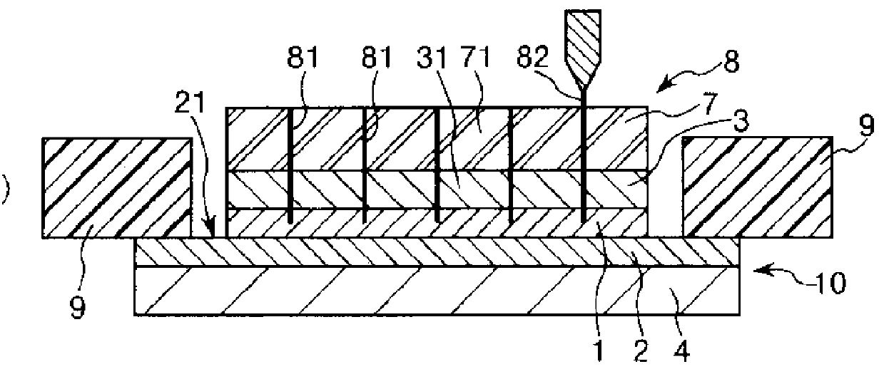
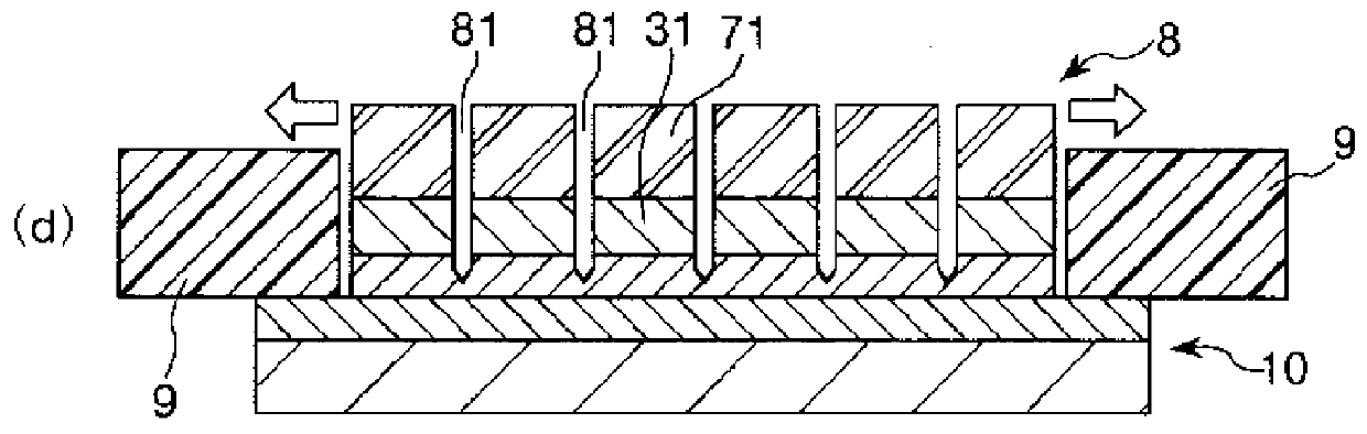
[0050]First, description will be made on a first embodiment of the film for semiconductor of the present invention and the method for manufacturing a semiconductor device of the present invention.
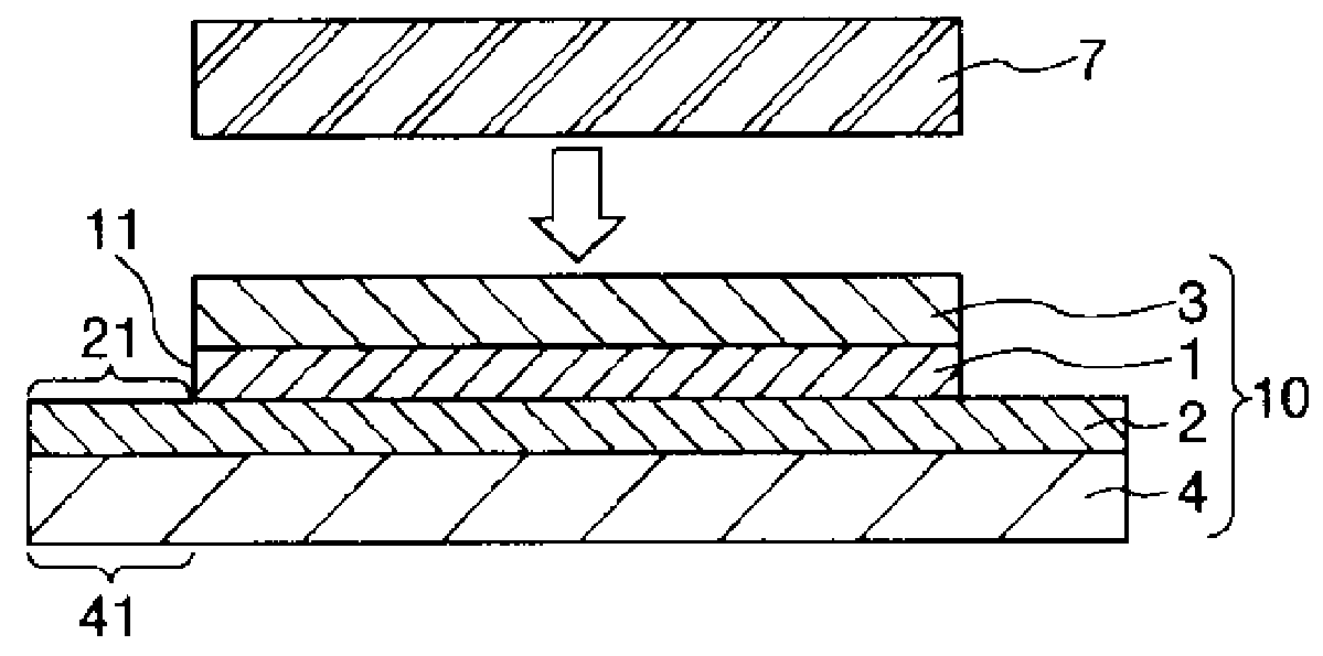
[0051]Each of FIGS. 1 to 3 is a view (sectional view) for explaining the first embodiment of the film for semiconductor of the present invention and the method for manufacturing a semiconductor device of the present invention, and FIG. 4 is a view for explaining a method for producing the film for semiconductor of the present invention. In this regard, in the following description, the upper side in each of FIGS. 1 to 4 will be referred to as “upper” and the lower side thereof will be referred to as “lower”.
[0053]A film for semiconductor 10 shown in FIG. 1 includes a support film 4, a first adhesive layer 1, a second adhesive layer 2 and a bonding layer 3. More specifically, in the film for semiconductor 10, the second layer 2, the first layer 1 and the bonding...
second embodiment
[0250]Next, description will be made on a second embodiment of the film for semiconductor of the present invention and the method for manufacturing a semiconductor device of the present invention.
[0251]FIG. 5 is a view (sectional view) for explaining the second embodiment of the film for semiconductor of the present invention and the method for manufacturing a semiconductor device of the present invention. In this regard, in the following description, the upper side in FIG. 5 will be referred to as “upper” and the lower side thereof will be referred to as “lower”.
[0252]Hereinbelow, the second embodiment will be described with emphasis placed on points differing from the first embodiment. No description will be made on the same points. In this regard, it is to be noted that the same reference numbers earlier described in FIG. 1 are applied to the same components shown in FIG. 5 as those of the first embodiment.
[0253]A film for semiconductor 10′ according to this embodiment is the sam...
[0272]100 parts by weight of a copolymer having a weight average molecular weight of 300,000 which was obtained by polymerizing 30 wt % of 2-ethyl hexyl acrylate with 70 wt % of vinyl acetate, 45 parts by weight of a penta-functional acrylatemonomer having a molecular weight of 700, 5 parts by weight of 2,2-dimethoxy-2-phenyl acetophenone and 3 parts by weight of tolylene diisocyanate (“CORONATE T-100” produced by NIPPON POLYURETHANE INDUSTRY CORPORATION) were applied onto a polyester film having a thickness of 38 μm and subjected to a releasing treatment so that a thickness thereof after being dried would become 10 μm, and then dried at 80° C. for 5 minutes to obtain an application film. Thereafter, the obtained application film was irradiated with an ultravioletray having 500 mJ / cm2 to thereby form a first adhesive layer on the polyester film.
[0273]In this regard, it is to be noted that Shore D hardness of the obtained first adhesive layer was 4...
PUM
Property
Measurement
Unit
Temperature
aaaaa
aaaaa
Temperature
aaaaa
aaaaa
Temperature
aaaaa
aaaaa
Abstract
A film for semiconductor includes a support film, a second adhesive layer, a first adhesive layer and a bonding layer which are laminated together in this order. This film for semiconductor is configured so that it supports a semiconductorwafer laminated on the bonding layer thereof when the semiconductor wafer is diced and the bonding layer is selectively peeled off from the first adhesive layer when a chip is picked up. This film for semiconductor is characterized in that in the case where peel strength at 23° C. of the chip is defined as “F23 (cN / 25 mm)” and peel strength at 60° C. of the chip is defined as “F60 (cN / 25 mm)”, F23 is in the range of 10 to 80 and F60 / F23 is in the range of 0.3 to 5.5. This makes it possible to improve a pickup property of the chip, to thereby prevent generation of defects in a semiconductor element.
Description
TECHNICAL FIELD[0001]The present invention relates to a film for semiconductor and a semiconductor device manufacturing method (that is, a method for manufacturing a semiconductor device).BACKGROUND ART[0002]According to the recent trend of high functionality of electronic devices and expansion of their use to mobile applications, there is an increasing demand for developing a semiconductor device having high density and high integration. As a result, an IC package having high capacity and high density is developed.[0003]In a method for manufacturing the semiconductor device, a bonding sheet is, first, attached to a semiconductor wafer made of silicon, gallium, arsenic or the like, and then the semiconductor wafer is fixed using a wafer ring at a peripheral portion thereof and is diced (or segmented) into individual semiconductor elements during a dicing step.[0004]Next, an expanding step in which the semiconductor elements obtained by the dicing are separated from each other and a ...
Claims
Application Information
Patent Timeline
Application Date:The date an application was filed.
Publication Date:The date a patent or application was officially published.
First Publication Date:The earliest publication date of a patent with the same application number.
Issue Date:Publication date of the patent grant document.
PCT Entry Date:The Entry date of PCT National Phase.
Estimated Expiry Date:The statutory expiry date of a patent right according to the Patent Law, and it is the longest term of protection that the patent right can achieve without the termination of the patent right due to other reasons(Term extension factor has been taken into account ).
Invalid Date:Actual expiry date is based on effective date or publication date of legal transaction data of invalid patent.

