Current sampling circuit of metal oxide semiconductor field effect transistor (MOSFET) switch element

A switching element and current sampling technology, applied in the direction of measuring current/voltage, measuring electrical variables, measuring devices, etc., can solve the problem of unable to use MOSFET switching element current sampling circuit, etc., to improve the working voltage range, remove power loss, improve The effect of voltage difference

Active Publication Date: 2012-06-13
HANGZHOU SILAN MICROELECTRONICS
View PDF4 Cites 17 Cited by
  • Summary
  • Abstract
  • Description
  • Claims
  • Application Information

AI Technical Summary

Problems solved by technology

However, the packaging method is not suitable for adding sampling elements due to the limitation of packaging, so the above-mentioned current sampling circuit of MOSFET switching elements cannot be used.

Method used


Image

  • Current sampling circuit of metal oxide semiconductor field effect transistor (MOSFET) switch element
  • Current sampling circuit of metal oxide semiconductor field effect transistor (MOSFET) switch element
  • Current sampling circuit of metal oxide semiconductor field effect transistor (MOSFET) switch element

Examples


Embodiment Construction

[0062] The content of the present invention will be further described below in conjunction with the accompanying drawings.

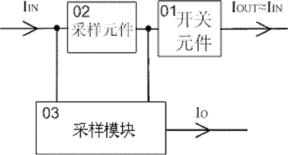
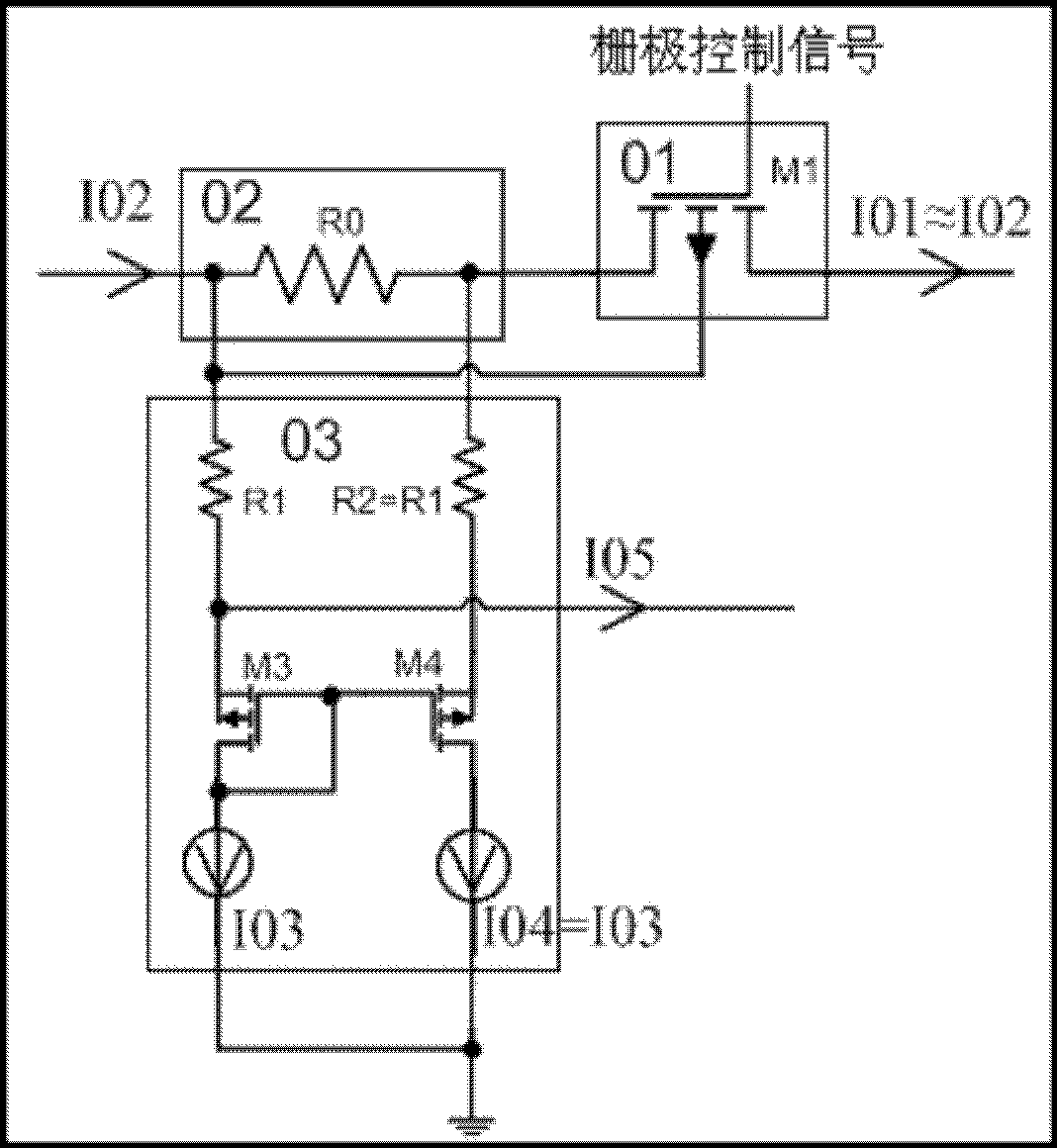
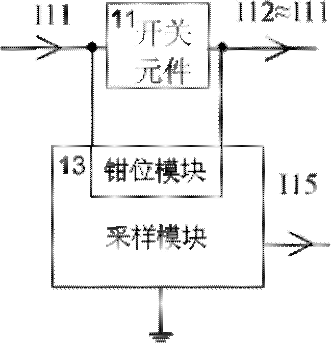
[0063] In order to solve the problem that the power loss of the current detection circuit of the traditional MOSFET switching element increases and the problem that the current detection circuit of the traditional MOSFET switching element cannot be applied to the integrated circuit of the drive control chip and the MOSFET switching element; the invention provides an improved MOSFET switching element The current sampling circuit directly samples the voltage difference between the first terminal and the second terminal of the MOSFET switching element, and the maximum allowable voltage difference between the first input terminal and the second input terminal of the sampling module is between the two input terminals of the sampling module The withstand voltage value between. When working at high voltage, due to the MOSFET switching element working in switch ...


PUM


Abstract

The invention discloses a current sampling circuit of a metal oxide semiconductor field effect transistor (MOSFET) switch element. A first end of the switch element is connected with a first input end of a sampling module and serves as a current input signal end, a second end of the switch element is connected with a second input end of the sampling module and serves as a current output signal end of the MOSFET switch element, and an output end of the sampling module serves as a sampling current output signal end. The sampling module directly samples voltage difference of the first end and the second end of the MOSFET switch element. Maximum voltage difference value allowed between the first input end and the second input end of the sampling module is a withstand voltage value between two input ends of the sampling module. A clamping module included in the sampling module increases the withstand voltage value of the sampling module so that a current path formed between the first input end and the second input end of the sampling module is blocked, and working voltage range of the current sampling circuit of the MOSFET switch element is improved.

Description

technical field [0001] The invention relates to a current sampling technology in a power management circuit, more precisely, to a technology and a current sampling circuit for sampling the current through the on-resistance of a MOSFET switching element. Background technique [0002] Power management circuits are widely used. Most power management circuits require built-in or external MOSFET switching elements, and detect the current value flowing through the MOSFET switching element to obtain a voltage signal or current signal related to the current value. According to the The voltage signal or the current signal controls the turn-on and turn-off of the MOSFET switching element. [0003] Figure 1A The current sampling circuit of a typical MOSFET switching element is shown, and the current value flowing through the MOSFET switching element 1 in the circuit is sampled: the switching element is a P-channel MOSFET switching element, and the first end of the MOSFET switching ele...

Claims


Application Information

Patent Timeline
Patent Type & Authority Applications(China)
IPC IPC(8): G01R19/00G01R15/00
Inventor 高阳吴剑辉
Owner HANGZHOU SILAN MICROELECTRONICS
Why Eureka
Try Eureka