
Planar waveguide, waveguide filter and antenna

A planar waveguide and waveguide technology, which is applied in waveguide filters, antennas, and planar waveguide fields, can solve problems such as rising costs, great influence on the impedance characteristics of microstrip lines, and reducing the pass-through rate.

Active Publication Date: 2012-06-13
HUAWEI TECH CO LTD
View PDF2 Cites 10 Cited by
  • Summary
  • Abstract
  • Description
  • Claims
  • Application Information

AI Technical Summary

Problems solved by technology

[0003] However, both of the above two methods of forming waveguides have certain limitations.
Among them, although the waveguide formed by the PCB microstrip line is simple to process and low in cost, the loss of the signal is large in the frequency band above 40 GHz, and the impedance characteristic of the microstrip line is affected by the size due to the high dielectric constant of the PCB medium. The impact is greater, resulting in high processing accuracy for PCBs, which increases the cost significantly, and also reduces the straight-through rate
Although the rectangular or circular waveguide formed by the metal cavity has very low signal loss, but in the frequency band above 40 GHz, the machining accuracy tolerance of the metal cavity reaches the micron level, and the shape is all three-dimensional, so it is necessary to use extremely high-precision Mold and processing technology, resulting in a substantial increase in cost

Method used


Image

  • Planar waveguide, waveguide filter and antenna
  • Planar waveguide, waveguide filter and antenna
  • Planar waveguide, waveguide filter and antenna

Examples


Embodiment Construction

[0022] In order to make the purpose, technical solutions and advantages of the embodiments of the present invention clearer, the technical solutions in the embodiments of the present invention will be clearly and completely described below in conjunction with the drawings in the embodiments of the present invention. Obviously, the described embodiments It is a part of embodiments of the present invention, but not all embodiments. Based on the embodiments of the present invention, all other embodiments obtained by persons of ordinary skill in the art without creative efforts fall within the protection scope of the present invention.

[0023] A waveguide is a structure used to confine or guide electromagnetic waves. The waveguide can confine and guide the electromagnetic wave to propagate in the length direction of the waveguide. Typically, off-the-shelf devices such as filters or antennas can be made, relying on this property of waveguides. Of course, the waveguide can also be...


PUM


Abstract

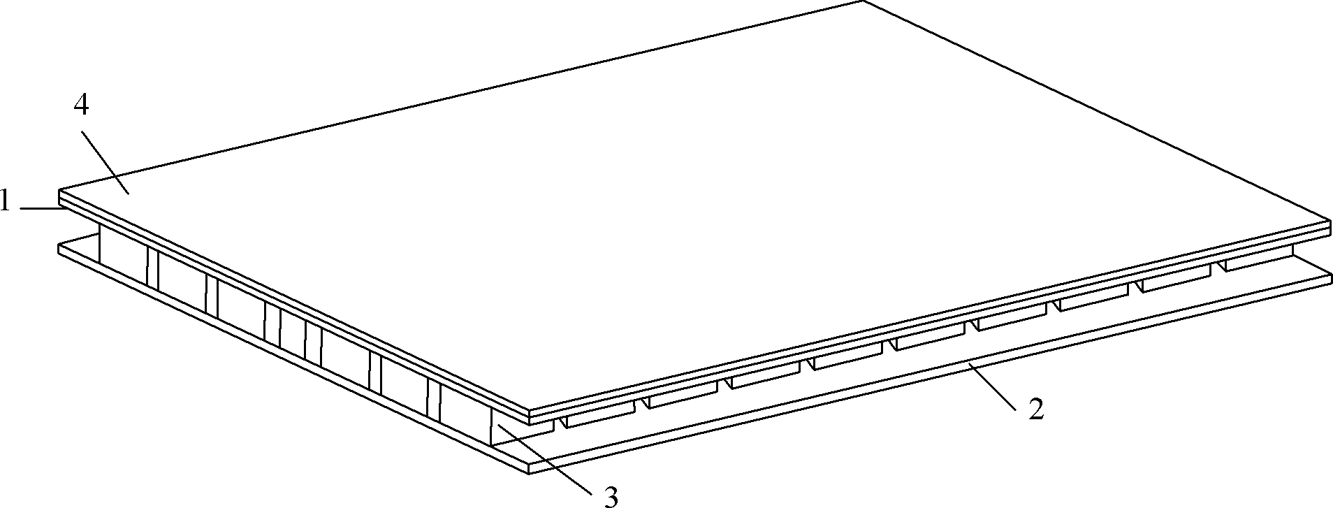
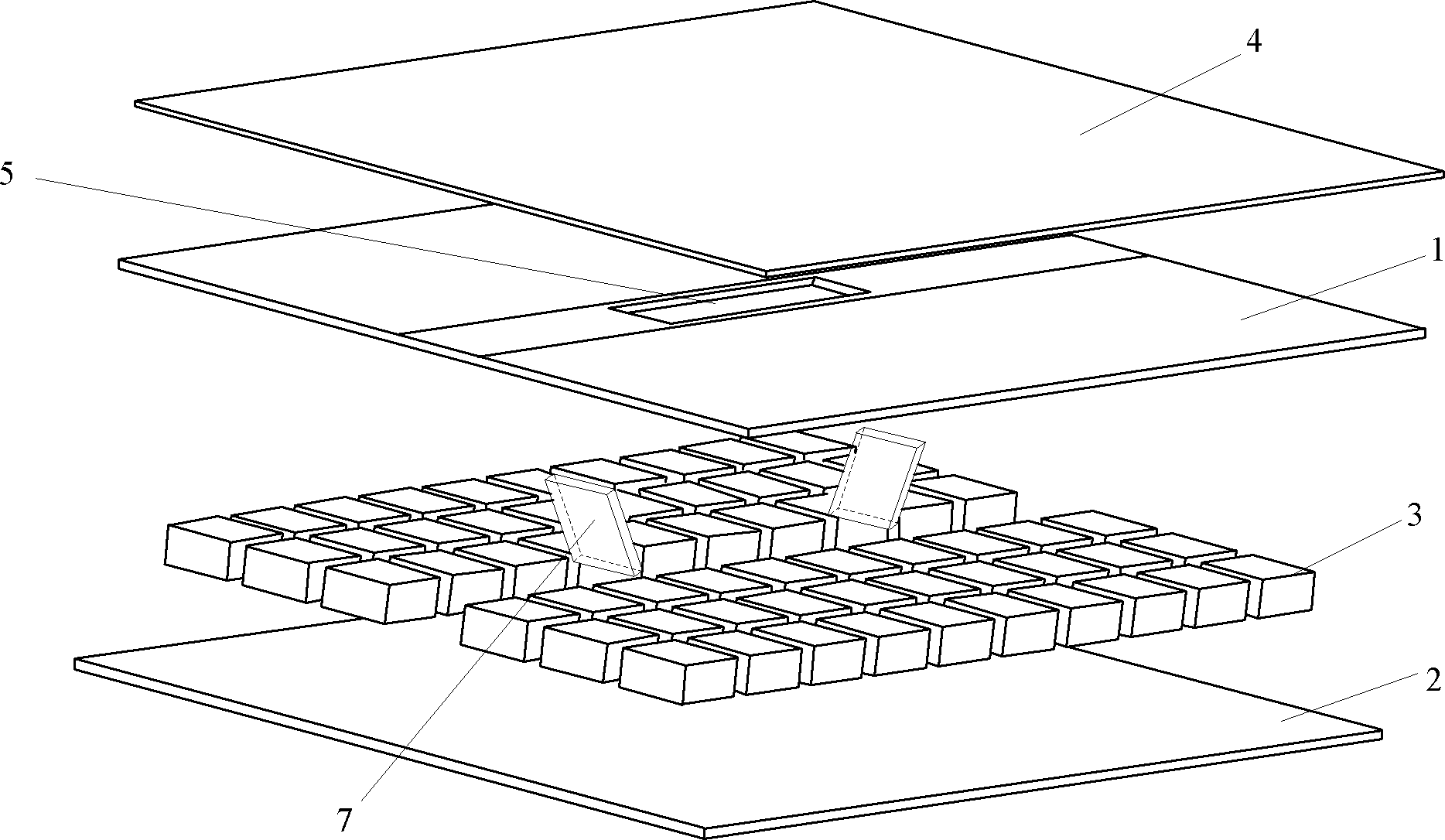
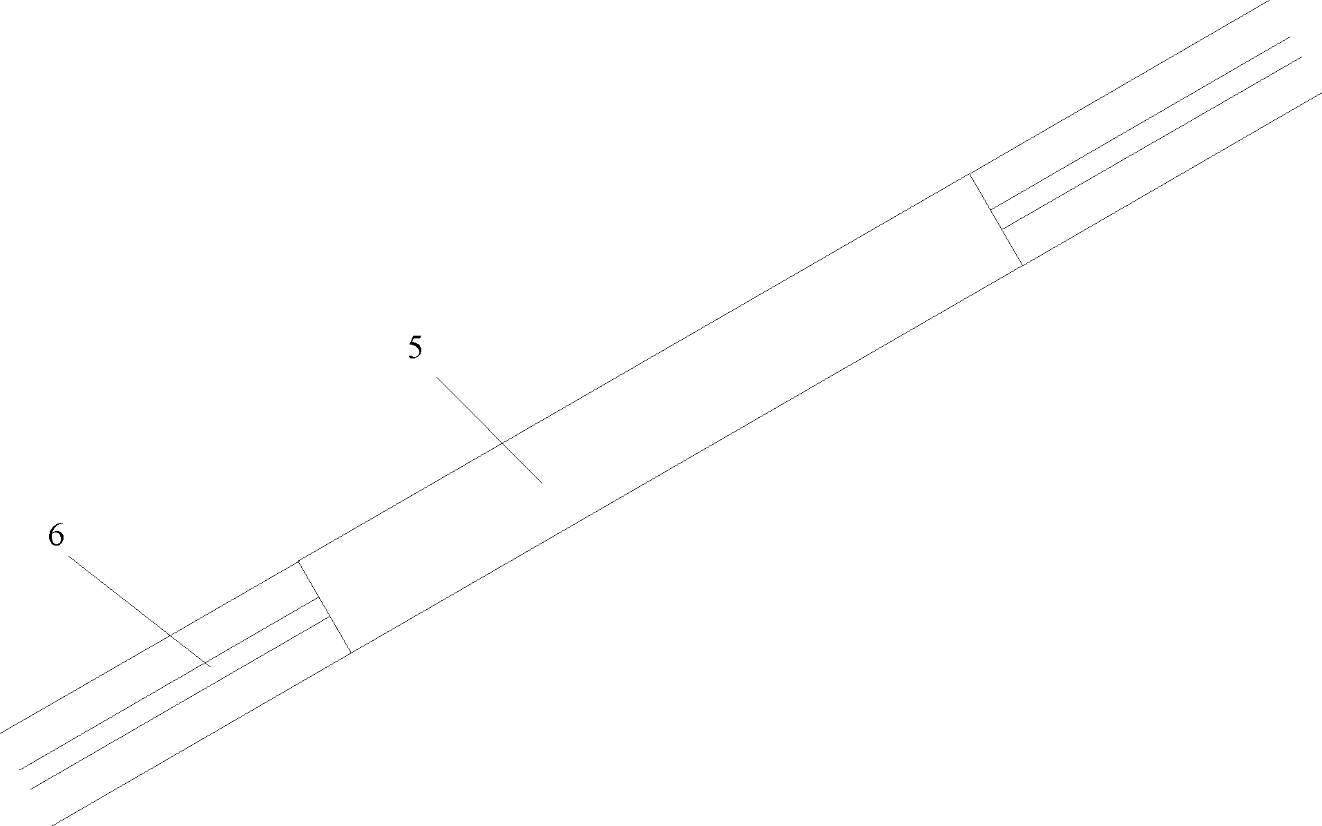
The invention provides a planar waveguide, a waveguide filter and an antenna. The planar waveguide comprises a top printed circuit board (PCB), a bottom PCB, a plurality of shielding metal blocks, and a metal plate. A groove is opened at the top PCB, an air waveguide is formed by the grooved and the bottom PCB; and microstrip lines are arranged at the lower surface of the top PCB. The microstrip lines are at two ends of the groove and are arranged along extending lines of the groove. The plurality of shielding metal blocks are arranged along the microstrip lines and extended directions of the groove as well as are arranged at two sides of the microstrip lines and the groove. A first conversion part that is used for realizing signal transmission between the microstrip lines and the air waveguide is arranged between the microstrip lines and the bottom PCB below the groove. And working gravity frequency of the planar waveguide is f0; and under the frequency of the f0, a wavelength lambda of an electromagnetic wave in the air satisfies the following relationship: lambda = c / f0; the height Hb of one of the shielding metal blocks satisfies the following relationship: 0.75*lambda <= Hb <= 1.25*lambda / 4; the width Wb satisfies the following relationship: lambda / 8 <= Wb <= lambda; and a gap Wg between each two of the shielding metal blocks satisfies the following relationship: 0 <= Wg <= lambda / 2.

Description

technical field [0001] The embodiments of the present invention relate to the technical field of wireless communication, and in particular to a planar waveguide, a waveguide filter, and an antenna. Background technique [0002] A waveguide is a conduit that confines and guides electromagnetic waves that propagate along their length. In microwave line electronic equipment, in order to control the conduction path of the microwave control signal, a waveguide formed by a printed circuit board (Printed Circuit Board, referred to as: PCB) microstrip line or a waveguide formed by a metal cavity is usually used, and through Control and change the shape of the microstrip line or the shape of the metal cavity to achieve functions such as filtering, power splitting and combining, and coupling of microwave signals. [0003] However, both of the above two methods for forming waveguides have certain limitations. Among them, although the waveguide formed by the PCB microstrip line is sim...

Claims


Application Information

Patent Timeline
Patent Type & Authority Applications(China)
IPC IPC(8): H01P3/00H01P1/20H01Q13/22
CPCH01P3/00H01P1/20H01Q13/22H01P3/084H01P5/08H01Q13/106
Inventor 欧健
Owner HUAWEI TECH CO LTD
Learn More