

Wafer chamfering machine and wafer machining method
A technology of chamfering machine and wafer, which is applied in the direction of metal processing equipment, manufacturing tools, grinding machine parts, etc., can solve the problems of high precision chamfering size, low manual processing precision, high labor cost, etc., to achieve High processing precision, improve the utilization rate of machinery, and avoid the effect of duplication of labor force
- Summary
- Abstract
- Description
- Claims
- Application Information
AI Technical Summary
Problems solved by technology
Method used
Image


Examples
Embodiment Construction
[0022] The present invention will be described in detail below in conjunction with the accompanying drawings. As a part of this specification, the principle of the present invention will be described through embodiments. Other aspects, features and advantages of the present invention will become clear at a glance through the detailed description.
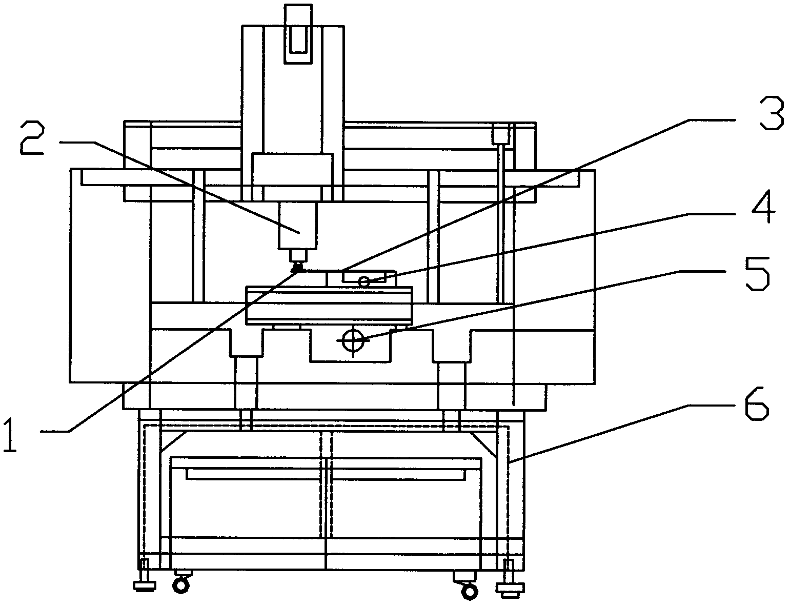
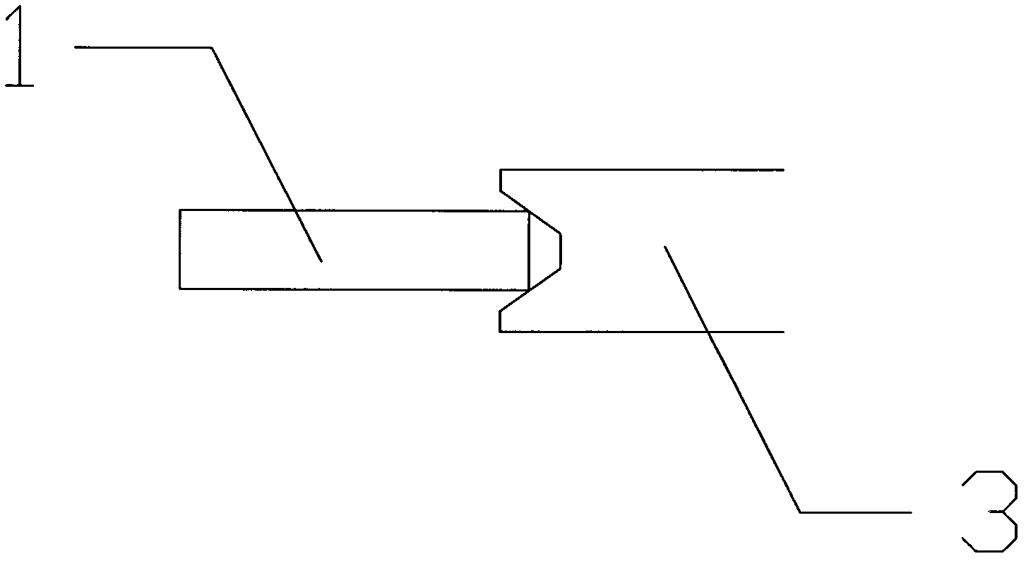
[0023] A wafer chamfering machine, including a frame 6, a data processing system and a numerical control device for processing wafers 3; the numerical control device includes a chamfering working end 1; the data processing system includes a data input unit, a data processing unit and Data output unit; the data output unit is connected with the numerical control device for inputting data to the numerical control device; the numerical control device is used to control the chamfering working end 1 to chamfer the wafer 3 .
[0024] The wafer chamfering machine adopts natural granite base, gantry frame, durable, no deformation, no vibrati...
PUM
 Abstract
Description
Claims
Application Information