Semiconductor material of Cu2O porous micro/nano cube and preparation method thereof
A nano-cube, semiconductor technology, applied in the direction of nanotechnology, can solve the problems of low cost, high cost, low success rate, etc.
- Summary
- Abstract
- Description
- Claims
- Application Information
AI Technical Summary
Problems solved by technology
Method used
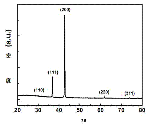
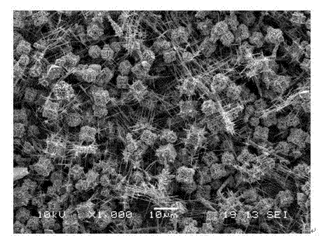
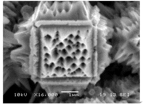
Image

Examples
Embodiment 1
[0032] 1. Clean the silicon wafer, and then cut it into small pieces of about 5mm×5mm;
[0033] 2. Set the temperature of the heating furnace to 180°C;
[0034] 3. Mix absolute ethanol and deionized water in a ratio of 1:3 and stir evenly as a solvent for later use;
[0035] 4. Add 0.5g of Cu(CH3 COO) 2 ·H 2 O powder was added to 100mL of the above-mentioned mixed solvent of absolute ethanol and deionized water to make Cu(CH 3 COO) 2 ·H 2 O content is the mixed solution of 25mM; Cu(CH 3 COO) 2 ·H 2 The O content allows an error of up and down 2.5mM, which has no effect on the reaction result;
[0036] 5. After stirring for about 5 minutes, add 1 mL of pyrrole dropwise to the above solution while stirring, Cu(CH 3 COO) 2 ·H 2 The molar ratio of O powder to pyrrole is 2:7, and the prepared reaction solution is light blue;
[0037] 6. Clean the Teflon reactor with a capacity of 100mL, place the cleaned silicon wafer horizontally on the bottom of the inner tank of the ...
PUM
 Abstract
Description
Claims
Application Information