Device for detecting in-plane error in micro/nano device out-of-plane motion test and compensating method

A motion error and motion measurement technology, which is applied in the direction of measuring devices, optical devices, instruments, etc., can solve problems affecting the reliability of measurement results, etc., and achieve the effects of avoiding errors, simple use, and high precision

Inactive Publication Date: 2012-06-20
TIANJIN UNIV
View PDF1 Cites 15 Cited by
  • Summary
  • Abstract
  • Description
  • Claims
  • Application Information

AI Technical Summary

Problems solved by technology

However, the in-plane motion test requires a bright-field image of the device, that is, a non-interference image. If the secondary measurement is performed under non-interference conditions, various uncertainties will be brought about due to the influence of the device itself, system and environmental factors, which will affect the measurement results. credibility

Method used


Image

  • Device for detecting in-plane error in micro/nano device out-of-plane motion test and compensating method
  • Device for detecting in-plane error in micro/nano device out-of-plane motion test and compensating method
  • Device for detecting in-plane error in micro/nano device out-of-plane motion test and compensating method

Examples


Embodiment Construction

[0039] The in-plane motion error detection device and compensation method in the out-of-plane motion measurement of the micro-nano device of the present invention will be described in detail below with reference to the embodiments and the accompanying drawings.

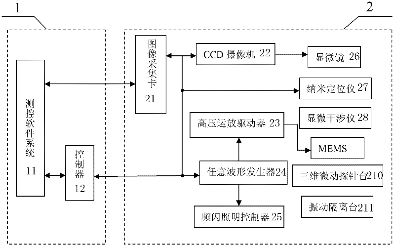
[0040] Such as figure 1 As shown, the in-plane motion error detection device in the out-of-plane motion measurement of micro-nano devices of the present invention has a control and image processing unit 1, and a phase-shift micro-interference system 2 connected to the control and image processing unit 1 , wherein, the control and image processing unit 1 is composed of a computer, and the phase-shift micro-interference system 2 includes:

[0041] Sequentially set up for obtaining the image of the micro-nano device 29 under test: a vibration isolation table 211, a three-dimensional micro-motion probe station 210, a micro-nano device under test 29, a micro-interferometer 28, a nanopositioner 27 and a microscope 26;

[0...


PUM


Abstract

The invention discloses a device for detecting an in-plane error in a micro/nano device out-of-plane motion test and a compensating method. The device has a control and image processing unit and a phase shift micro interfering system which is connected with the control and image processing unit, wherein the phase shift micro interfering system comprises a vibration isolating table, a three-dimensional micro motion probe table, a tested micro/nano device, a micro interferometer, a nano positioning instrument and a microscope, which are arranged in turn, and a flash lighting controller, a high-pressure amplifier driver, an arbitrary waveform generator, a charged coupled device (CCD) camera, and an image acquisition card; the input end of the arbitrary waveform generator is connected with the control and image processing unit, and the output end of the arbitrary waveform generator is connected with the flash lighting controller and the high-pressure amplifier driver; the CCD camera is connected with a microscope; and the image acquisition card is connected with the control and image processing unit and the CCD camera respectively. The method comprises: acquiring the motion image of the tested micro/nano device; testing in-plane displacement; testing out-of-plane motion; and performing two-phase unwrapping of a time axis and a spatial axis. The invention is easy to use with high reliability.

Description

technical field [0001] The invention relates to a motion error compensation method. In particular, it relates to an in-plane motion error detection device and compensation method in out-of-plane motion measurement of micro-nano devices. Background technique [0002] Micro / Nano ElectroMechanical System (MEMS / NEMS) is an integrated microsystem integrating sensing, information processing and execution. In recent years, it has become an important high-tech field and a research hotspot, and its research and development hotspots include sensing, actuation, radio frequency (RF), optics, biochemistry, military, aerospace and medical devices. The feature size of these devices is micron and nanometer level, and its strong vitality lies in small volume, large batch, low cost and high reliability, which makes MEMS / NEMS have a wide range of application prospects. MEMS has become one of the most promising scientific research fields in the 21st century. Its rapid development has put forw...

Claims


Application Information

Patent Timeline
Patent Type & Authority Applications(China)
IPC IPC(8): G01B11/00
Inventor 陈治陈澄李艳宁丹特・多伦雷傅星胡小唐
Owner TIANJIN UNIV
Why Eureka
Try Eureka