Small-sized substrate integrated waveguide band-pass hybrid ring
A substrate-integrated waveguide and hybrid ring technology, applied in waveguide-type devices, electrical components, connection devices, etc., can solve the problems of complex system framework, large circuit area, large loss, etc., to reduce circuit area, compact layout, avoid The effect of wasting interior space
- Summary
- Abstract
- Description
- Claims
- Application Information
AI Technical Summary
Problems solved by technology
Method used
Image

Examples
Embodiment 1
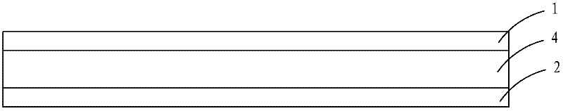
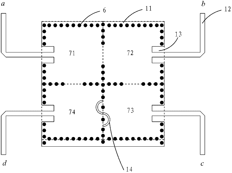
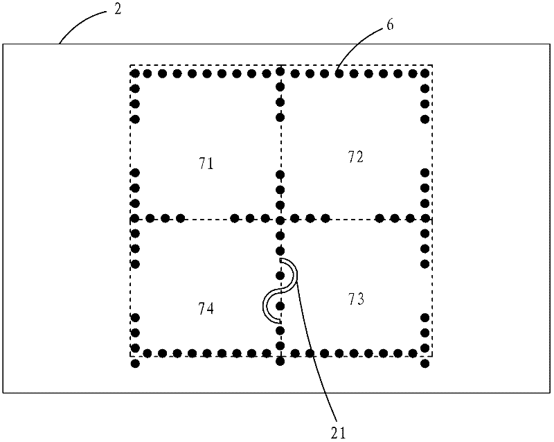
[0018] Embodiment 1: as figure 1 , figure 2 , image 3 As shown, a substrate-integrated waveguide miniaturized bandpass hybrid ring includes a first metal copper clad layer 1, a dielectric layer 4, and a second metal copper clad layer 2 stacked sequentially from top to bottom, in order to form the hybrid ring of the present invention , the first metal copper clad layer 1 and the second metal copper clad layer 2 are processed through the printed circuit board manufacturing process to form the required metal pattern (circuit structure), and the parts in the pattern are divided by virtual dotted lines , punch holes in the dielectric layer 4 and perform surface metallization treatment on the holes to form metallized through holes 6, the first metal copper clad layer 1 includes the upper surface area 11 of the substrate integrated waveguide, and is located on the upper surface area 11 of the substrate integrated waveguide Four microstrip lines 12 on both sides and connected ther...
Embodiment 2
[0027] Embodiment 2: as Figure 4 , Figure 5 , Image 6 As shown, a substrate-integrated waveguide miniaturized bandpass hybrid ring includes a first metal copper clad layer 1, a dielectric layer 4, a second metal copper clad layer 2, a second dielectric layer 5, a The three metal copper clad layers 3 are formed by processing the first metal copper clad layer 1, the second metal copper clad layer 2 and the third metal copper clad layer 3 through the printed circuit board manufacturing process in order to form the hybrid ring of the present invention. The required metal pattern (circuit structure), each part of the pattern is divided by a virtual dotted line, the dielectric layer 4 and the second dielectric layer 5 are punched and the holes are subjected to surface metallization treatment to form a metallized through hole 6, The first metal copper clad layer 1 includes the upper surface area 11 of the substrate integrated waveguide, two microstrip lines 12 located on both si...
PUM
 Abstract
Description
Claims
Application Information
 - Generate Ideas
- Intellectual Property
- Life Sciences
- Materials
- Tech Scout
- Unparalleled Data Quality
- Higher Quality Content
- 60% Fewer Hallucinations
Browse by: Latest US Patents, China's latest patents, Technical Efficacy Thesaurus, Application Domain, Technology Topic, Popular Technical Reports.
© 2025 PatSnap. All rights reserved.Legal|Privacy policy|Modern Slavery Act Transparency Statement|Sitemap|About US| Contact US: help@patsnap.com