
Optical waveguide element

An optical waveguide and waveguide technology, applied in optical components, optical waveguides, light guides, etc., can solve problems such as the deterioration of extinction ratio, and achieve the effect of suppressing absorption and improving on/off extinction ratio.

Inactive Publication Date: 2012-06-20
SUMITOMO OSAKA CEMENT CO LTD
View PDF7 Cites 5 Cited by
  • Summary
  • Abstract
  • Description
  • Claims
  • Application Information

AI Technical Summary

Problems solved by technology

Therefore, the extinction ratio may deteriorate due to the applied voltage
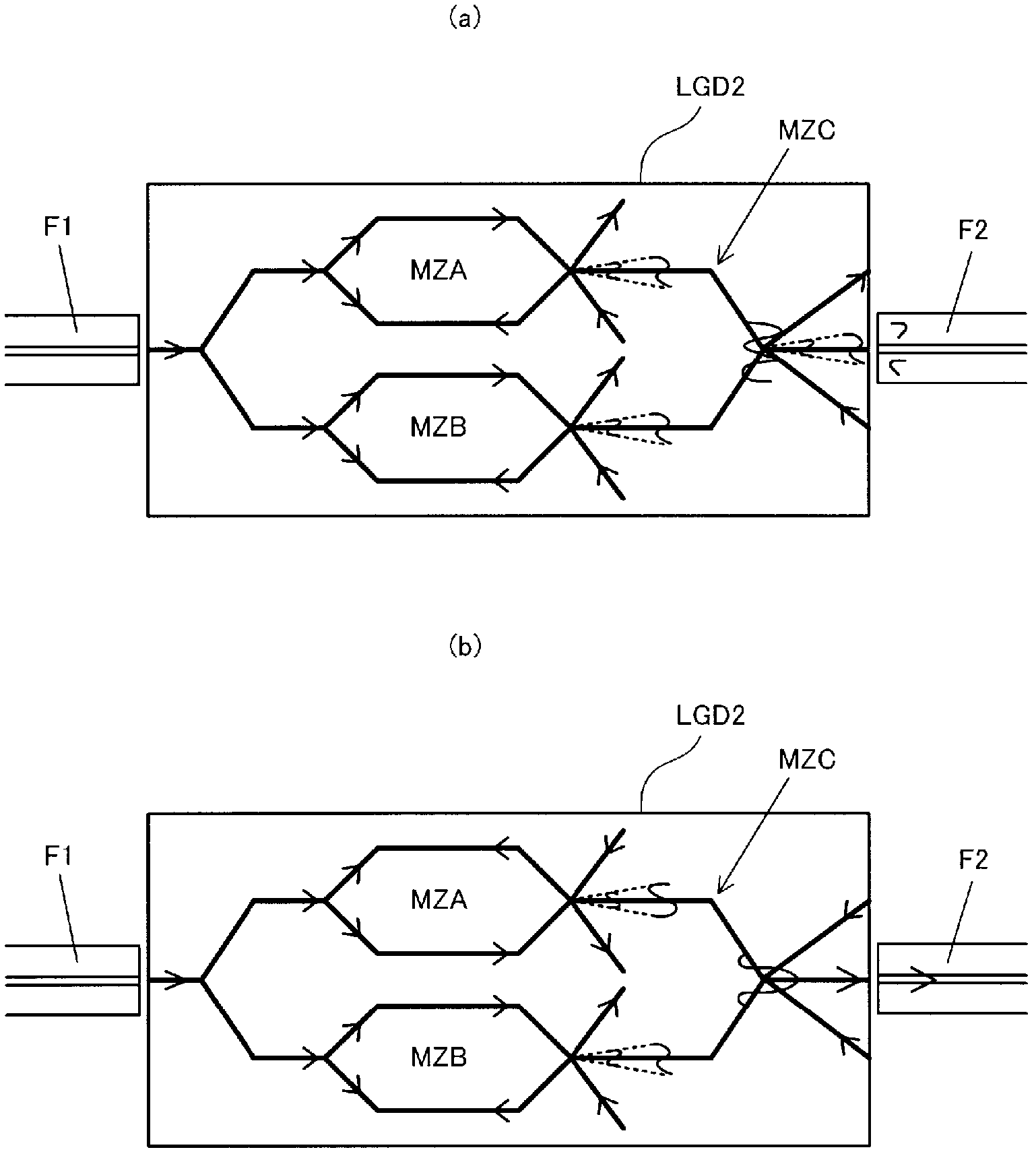
This is easy to occur when the MZ-type waveguide is integrated using a thin plate structure, and cannot be solved by using a three-branch structure as in Patent Document 1.

Method used


Image

  • Optical waveguide element
  • Optical waveguide element
  • Optical waveguide element

Examples


Embodiment Construction

[0037] Hereinafter, the optical waveguide element of the present invention will be described in detail using preferred examples.

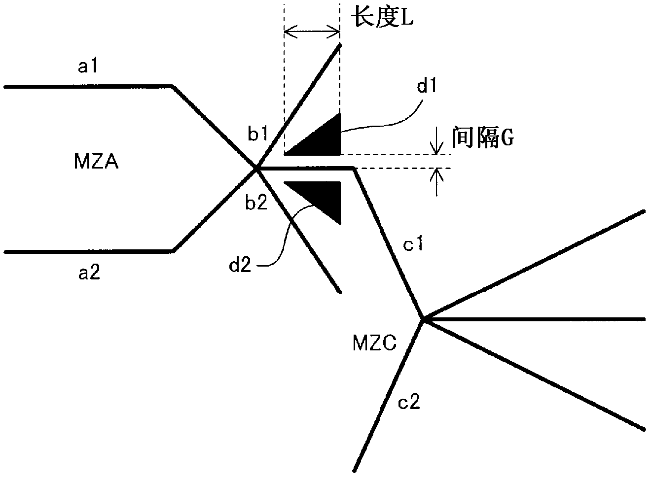
[0038] like image 3 As shown, the optical waveguide element of the present invention includes a thin plate with a thickness of 20 μm or less formed of a material having an electro-optical effect and an optical waveguide formed on the front or back of the thin plate. The optical waveguide element is characterized in that the optical waveguide has a plurality of Mach-Zehnder type waveguides, and the optical waves output from at least two or more Mach-Zehnder type waveguides are combined, and the multiplexer in this Mach-Zehnder type waveguide (MZA) is formed by A three-branched waveguide composed of an output waveguide (c1) and two radiated light waveguides (b1, b2) disposed so as to sandwich the output waveguide. Higher-order mode light absorption regions (d1, d2) are formed between the waveguides.

[0039]As a material having an electro-optical ...


PUM

PropertyMeasurementUnit
thicknessaaaaaaaaaa
lengthaaaaaaaaaa
lengthaaaaaaaaaa

Abstract

Disclosed is an optical waveguide element wherein a plurality of Mach-Zehnder waveguides to be used for DQPSK modulation and the like are integrated on a thin substrate and the on / off extinction ratio is improved. The optical waveguide element has the thin board, which is formed of a material having electrooptical effects and has a thickness of 20 [mu]m or less, and an optical waveguide formed on the front surface or the rear surface of the thin board. The optical waveguide has the plurality of Mach-Zehnder waveguide sections, and multiplexes optical waves outputted from two or more Mach-Zehnder waveguide sections. In the multiplexing section in each Mach-Zehnder waveguide section (MZA), a triply branched waveguide, which is composed of a waveguide for output (c1) and two waveguides for radiation (b1, b2) disposed to sandwich the waveguide for output, is formed. High-order mode light absorption regions (d1, d2) are formed between the waveguide for output and the waveguides for radiation in the triply branched waveguide.

Description

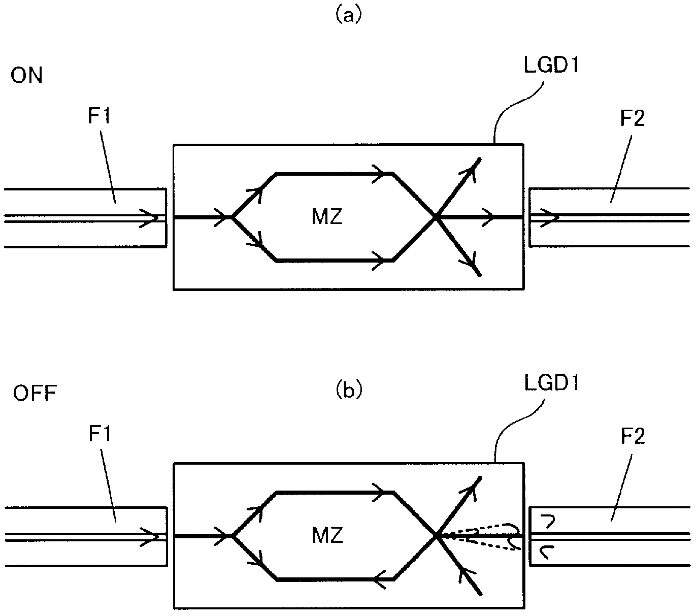
technical field [0001] The present invention relates to optical waveguide elements used in optical communication and optical information processing, and in particular to integration of multiple Mach-Zehnder waveguides on a thin substrate used in DQPSK modulation and the like optical waveguide components. Background technique [0002] Existing optical modulators in which optical waveguides are formed on substrates such as lithium niobate (LN) figure 1 As shown, the shape of the waveguide is formed as a Mach-Zehnder (MZ) type structure, and the intensity modulation is dominant. The optical modulator of the MZ type structure has modulation electrodes arranged along the MZ type waveguide, and the on (turn-on) / off (cut-off) of light is controlled by the voltage applied to the modulation electrodes. [0003] Specifically, the light can be turned on / off by fundamental mode-excitation mode control based on the MZ-type waveguide, where the output waveguide is a single-mode waveguid...

Claims


Application Information

Patent Timeline
Patent Type & Authority Applications(China)
IPC IPC(8): G02F1/035G02B6/12
CPCG02B6/14G02B6/12007G02F2201/08G02F1/225G02B6/12G02F1/035
Inventor 近藤胜利
Owner SUMITOMO OSAKA CEMENT CO LTD
Learn More