e/LQFP (low-profile quad flat package) stacked package with grounded ring and production method of e/LQFP stacked package with grounded ring
A production method and grounding ring technology, applied in semiconductor/solid-state device manufacturing, semiconductor/solid-state device parts, electrical components, etc., can solve the problems of easy-to-scan delamination, large chip bonding, non-stick carrier silver plating area, etc. Problems, to achieve the effect of improving reliability and test yield, increasing binding force, high reliability and test yield
- Summary
- Abstract
- Description
- Claims
- Application Information
AI Technical Summary
Problems solved by technology
Method used
Image
Examples
Embodiment 1
[0081] The wafer is thinned by the existing process method to obtain a thinned wafer with a final thinned thickness of 150 μm; during the thinning process, the rough grinding speed is 5 μm / s, and the thickness of the wafer after rough grinding is 200 μm + film thickness; The fine grinding speed is 0.5μm / s, and the thickness of the wafer after fine grinding is the final thinning thickness of the wafer + the thickness of the adhesive film. The process of preventing chip warpage is adopted during thinning. Use DISC 3350 dicing machine for scribing; when scribing, control the scribing feed speed to ≤10mm / s, and use anti-fragmentation and anti-crack scribing process software control technology;
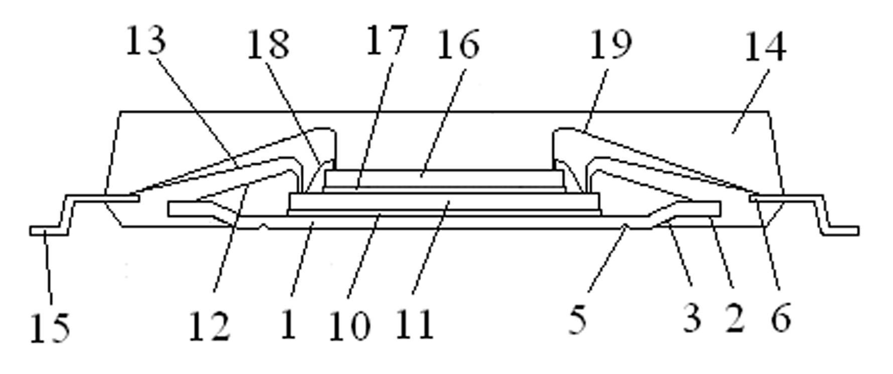
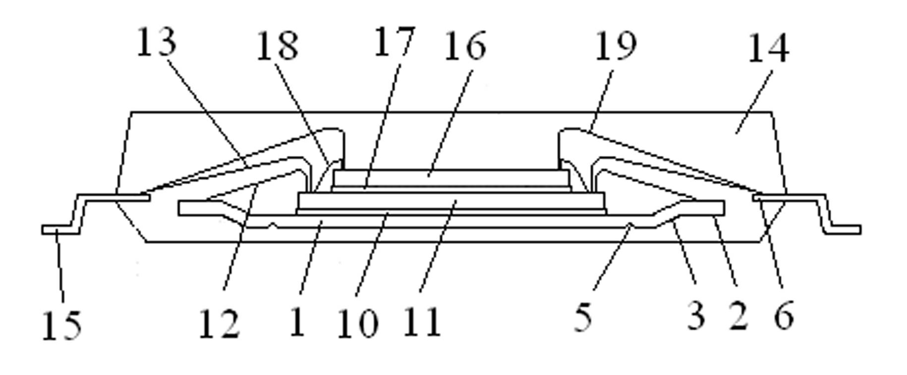
[0082] The difference between the side length of the first IC chip 11 and the side length of the second IC chip 16 is greater than 1.2mm. Two times of core loading and one baking are adopted: when the core is loaded for the first time, a lead frame with a grounding ring is used, and the lea...
Embodiment 2
[0084] The wafer is thinned by the existing process method to obtain a thinned wafer with a final thinned thickness of 200 μm; during the thinning process, the rough grinding speed is 3 μm / s, and the thickness of the wafer after rough grinding is 250 μm + film thickness; The fine grinding speed is 0.75μm / s, and the thickness of the wafer after fine grinding is the final thinning thickness of the wafer + the thickness of the adhesive film. , control the scribing feed speed ≤ 10mm / s, and adopt anti-fragmentation, anti-crack scribing process software control technology. The difference between the side length of the first IC chip 11 and the side length of the second IC chip 16 is equal to 1.2mm. Two times of core loading and one baking are adopted: when the core is loaded for the first time, a lead frame with a ground ring is used, and the lead frame with the ground ring is used. The lead frame is sent to the feeding table, and the chip bonder grabs a lead frame and sends it into ...
Embodiment 3
[0086] The wafer is thinned by the existing process method to obtain a thinned wafer with a final thinning thickness of 180 μm; during the thinning process, the rough grinding speed is 4 μm / s, and the thickness of the wafer after rough grinding is the final thinning thickness of the wafer. Thickness + adhesive film thickness + 50μm; fine grinding speed 1.0μmum / s, the wafer thickness after fine grinding is the final wafer thinning thickness + adhesive film thickness, and the chip warpage prevention process is adopted during thinning. A-WD-300TXB dicing machine is used for scribing; when scribing, the scribing feed speed is controlled to be ≤10mm / s, and the anti-fragment and anti-crack scribing process software control technology is adopted. The difference between the side length of the first IC chip 11 and the side length of the second IC chip 16 is less than 1.2 mm. Two times of core loading and two times of baking are used: when the first core is loaded, a lead frame with a gr...
PUM
 Abstract
Description
Claims
Application Information


