Schottky barrier diode rectifying device and manufacture method thereof

A diode rectification and Schottky potential technology, applied in semiconductor/solid-state device manufacturing, semiconductor devices, electrical components, etc., can solve the problem that the gap filling ability of the upper metal layer material is not good, and the surrounding area of ​​the electric field intensity curve does not change significantly. Device reliability and other issues

Inactive Publication Date: 2012-06-27
SUZHOU SILIKRON SEMICON CO LTD
View PDF5 Cites 1 Cited by
  • Summary
  • Abstract
  • Description
  • Claims
  • Application Information

AI Technical Summary

Problems solved by technology

[0005] However, the main problem exposed by the existing technology structure is the limited improvement of the reverse voltage blocking ability of the device
like figure 2 As shown in the middle electric field strength curve, the position of the peak value of the electric field strength changes with the depth of the trench, but the area surrounded by the electric field strength curve do

Method used


Image

  • Schottky barrier diode rectifying device and manufacture method thereof
  • Schottky barrier diode rectifying device and manufacture method thereof
  • Schottky barrier diode rectifying device and manufacture method thereof

Examples


Example Embodiment

[0039] Examples:

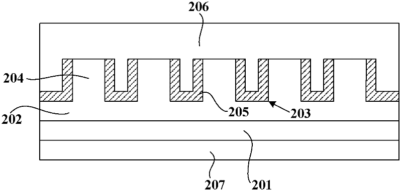
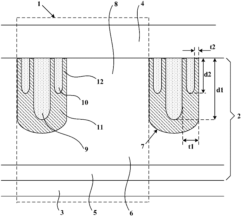
[0040] A Schottky barrier diode rectifier device, such as image 3 As shown, the active area of ​​the device is composed of a number of Schottky barrier diode cells 1 in parallel; in cross-section, each cell 1 includes a silicon wafer 2, and a lower metal layer 3 located on the back of the silicon wafer 2, The upper metal layer 4 located on the front side of the silicon wafer 2, the first conductive type heavily doped single crystal silicon substrate 5 connected to the lower metal layer 3 at the lower part of the silicon wafer 2, and the upper part of the silicon wafer 2 The first conductivity type lightly doped monocrystalline silicon epitaxial layer 6 connected to the upper metal layer 4 is located on the upper part of the epitaxial layer 6 and opens to the trench 7 on the upper surface of the epitaxial layer 6, adjacent to the trench 7 The boss 8 formed in the region of the epitaxial layer 6 between, the first conductive polysilicon region 9 heavily doped wi...


PUM


Abstract

The invention discloses a Schottky barrier diode rectifying device and a manufacture method thereof. According to the device, an active region is formed by parallel connection of a plurality of Schottky barrier diode unit cells; each unit cell comprises a first conductive light dope monocrystalline silicon epitaxial layer which is connected with an upper part of a silicon chip and an upper metal layer, grooves which are at an upper part of the epitaxial layer and whose openings are at upper surface of the epitaxial layer, and a boss which is formed between adjacent grooves in an epitaxial layer area; a lower metal layer and a substrate form ohmic contact; the upper metal layer is connected with upper surfaces of a first conductive polysilicon zone and a second conductive polysilicon zone to form ohmic contact; the upper metal layer is connected with an upper surface of the boss to form Schottky barrier contact; lower bottom depth of the first conductive polysilicon zone is larger than lower bottom depth of the second conductive polysilicon zone; and thickness of a first isolation oxidation layer is larger than thickness of the second isolation oxidation layer. According to the device and the method of the invention, reverse voltage blockout capability of the device is enhanced substantially, slit filling capability is improved, thus much flexibility is provided for device structure design, and device reliability is reinforced.

Description

technical field [0001] The invention relates to a rectifying device and a manufacturing method thereof, in particular to a Schottky barrier diode rectifying device and a manufacturing method thereof. Background technique [0002] As a conversion device from AC to DC, the rectifier device requires unidirectional conduction characteristics, that is, low turn-on voltage and small on-resistance during forward conduction, and high blocking voltage and low reverse leakage when reverse biased. Schottky barrier diodes have been used in power supply applications for decades as rectifying devices. Compared with PN junction diodes, Schottky barrier diodes have the advantages of low forward turn-on voltage and fast switching speed, which makes them very suitable for switching power supplies and high-frequency applications. [0003] Schottky barrier diodes are manufactured using the principle of a metal-semiconductor junction formed by contact between a metal and a semiconductor. The t...

Claims


Application Information

Patent Timeline
IPC IPC(8): H01L29/872H01L29/06H01L21/329
CPCH01L29/8725H01L29/66143
Inventor 刘伟王凡
Owner SUZHOU SILIKRON SEMICON CO LTD
Why Eureka
Try Eureka