A test head for automatic inspection of wafer-level packaging chips and its implementation method

A wafer-level packaging and test head technology, applied in the field of test heads, can solve the problems of high cost and low efficiency of manual test methods, achieve high test efficiency and meet the requirements of automated testing

Active Publication Date: 2015-07-29
CENT SOUTH UNIV
View PDF10 Cites 0 Cited by
  • Summary
  • Abstract
  • Description
  • Claims
  • Application Information

AI Technical Summary

Problems solved by technology

[0003] For the testing of wafer-level chip packaging products (such as wafer-level TSV through-silicon via 3D packaging), the usual test method: cut the packaged wafer into individual chips, manually put them into IC Socket (IC fixture) and press them. Tight testing, manual testing methods are inefficient and costly

Method used


Image

  • A test head for automatic inspection of wafer-level packaging chips and its implementation method
  • A test head for automatic inspection of wafer-level packaging chips and its implementation method
  • A test head for automatic inspection of wafer-level packaging chips and its implementation method

Examples


Embodiment Construction

[0026] The present invention will be described in further detail below in conjunction with accompanying drawing and specific embodiment:

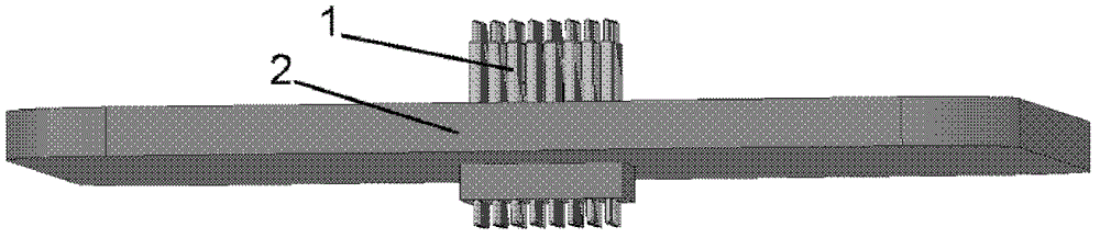
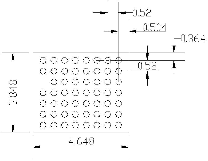
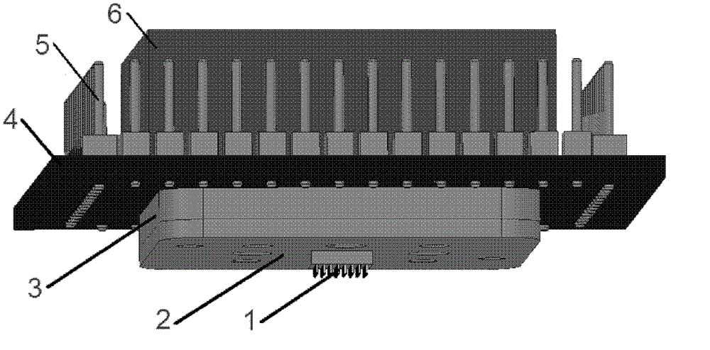
[0027] According to the test requirements of an IC chip, select the probe model, such as the selected probe is DE1-030EF40-010 double-headed probe, according to the package size and bump layout of a single IC chip on the wafer, such as figure 2 , design the corresponding fixed probes on the probe plate 2 of the array probe 1, such as image 3 , and then design the probe guide plate 3, (the specific structure of the probe guide plate is as follows Figure 4 As shown), in order to install and replace the probe array, design the PCB board 4, etch the connection point corresponding to the probe array 1 on the PCB board, and lead the wiring of the probe array to the periphery of the PCB through the wiring of the PCB board. And make the insertion pin 5, the signal of microarray probe test like this can be connected to the test box through the i...


PUM


Abstract

The invention discloses a test head for automatically detecting wafer-level packaged chips and an implementing method for the test head. The test head comprises a mounting plate, a printed circuit board (PCB), a plurality of plug wire pins, a probe guide plate and a probe plate; the probe plate is provided with a probe array; the mounting plate, the PCB, the probe guide plate and the probe plate are sequentially fixed together in a stacked mode, and the probe guide plate is arranged between the probe plate and the bottom of the PCB; and the plug wire pins are arranged on the top of the PCB, and the plug wire pins are electrically connected with the probe array through a printed circuit on the PCB. The test head for automatically detecting the wafer-level packaged chips and the implementing method for the test head can effectively improve the test efficiency of the wafer-level packaged chips based on an array probe test mode.

Description

technical field [0001] The invention relates to a test head used for automatic detection of wafer-level packaging chips and its realization method. Background technique [0002] Integrated circuit (IC) testing is juxtaposed with IC design, IC manufacturing and IC packaging, and constitutes the four pillars of the IC industry. The characteristic of the cost development of the semiconductor industry is that its unit function manufacturing cost decreases by an average of 25% to 30% per year, while the test cost increases by an average of 10.5% per year. As the number of functions per chip increases, it becomes increasingly difficult and expensive to test the final product. According to Moore's law of testing proposed by the president of Intel Corporation, the silicon investment cost of silicon transistors will be lower than its testing cost in the next few years. According to NTRS, by 2012 the price of testing a transistor may exceed the price of manufacturing a transistor. ...

Claims


Application Information

Patent Timeline
Patent Type & Authority Patents(China)
IPC IPC(8): G01R1/073G01R31/28
Inventor 李军辉邓路华刘灵刚韩雷王福亮
Owner CENT SOUTH UNIV
Why Eureka
Try Eureka