Wafer pre-alignment method

A pre-alignment, wafer technology, applied in the direction of electrical components, semiconductor/solid-state device manufacturing, circuits, etc., can solve the problems of accuracy impact, lack of robustness, and adjacent data amplitude cannot change too much, so as to avoid The effect of positioning error and avoiding influence

Inactive Publication Date: 2012-07-04
SHENYANG SIASUN ROBOT & AUTOMATION
View PDF2 Cites 14 Cited by
  • Summary
  • Abstract
  • Description
  • Claims
  • Application Information

AI Technical Summary

Problems solved by technology

Among the calculation methods of the center of the wafer, the radius of gyration method has a small amount of calculation, but it requires that the angles of the sampling points relative to the rotation center should be evenly distributed, and the total number of sampling points in a circle is a double-even number, which causes a lot of damage to the data collection of the sampling points. Difficult; although the calculation amount of the trajectory fitting method is small, the wafer is not a regular circle and has a gap, and the noise in the measurement process will affect the accuracy
[0004] Among the commonly used methods for wafer notch location, the edge change rate method calculates the angle between three adjacent sampling points and requires setting a suitable threshold. This threshold is mainly determined by empirical methods and does not have strong robustness. At the same time, this method requires that the amplitude of adjacent data collected cannot change too much

Method used


Image

  • Wafer pre-alignment method
  • Wafer pre-alignment method
  • Wafer pre-alignment method

Examples


Embodiment Construction

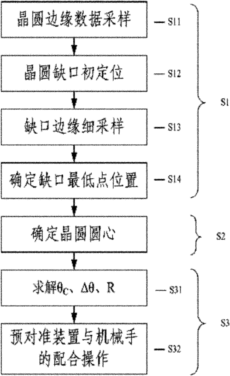
[0020] The method of the present invention is applied to a wafer pre-alignment device, and the wafer pre-alignment device has a rotary table, a CCD sensor, and cooperates with a corresponding IC robot to complete the pre-alignment operation of the wafer. figure 1 It is a diagram of the implementation steps of the wafer pre-alignment method of the present invention, mainly including the notch positioning step S1 of the wafer, the positioning step S2 of the center of the wafer, and the cooperative operation S3 of the pre-alignment device and the manipulator, as follows:

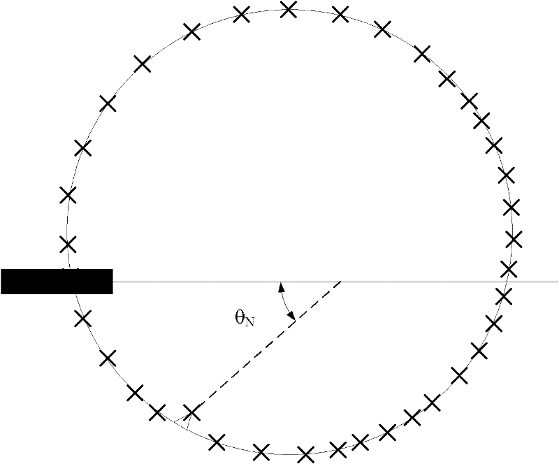
[0021] The wafer is driven to rotate through the rotary table, and the data of the edge of the wafer is collected by the CCD sensor, and the sampling data of the wafer is obtained;

[0022] Using the step drop method to determine the initial estimated position of the lowest point of the notch on the wafer sampling data;

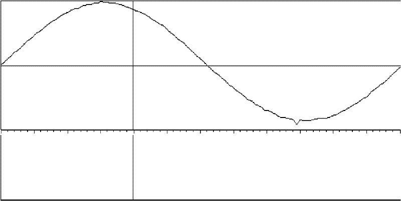
[0023] Rotate the wafer notch to the vicinity of the CCD sensor, and perform a small range...


PUM


Abstract

The invention relates to a wafer pre-alignment method. The wafer pre-alignment method comprises the following steps of: driving a wafer to rotate through a rotating table, collecting edge data of the wafer through a CCD (charge-coupled device) sensor to get sampled data on one circle of the wafer; determining an initial estimation position of a lowest point of a gap through a stepping fall method; rotating the gap of the wafer till being in the vicinity of the CCD sensor and performing small-range fine sampling on the edge of the gap; determining the position of the lowest point of the gap of the wafer through the stepping fall method; eliminating the sampled data in the range of the gap of the wafer from the sampled data on the edge of the wafer; fitting the center of a circle of the wafer from the sampled data on the edge of the wafer after eliminating the gap by applying a least square method; and solving the stop position of the rotating table, as well as the deflection angle and the extension distance of a mechanical arm of an IC (integrated circuit) robot and guiding the IC robot to move to an assigned position to take away the wafer. The wafer pre-alignment method disclosed by the invention is not limited by the size of the wafer and the shape of the gap, positioning errors caused by inaccurate setting of a threshold can be avoided, and the data at the gap can be prevented from affecting a fitting result.

Description

technical field [0001] The invention relates to a pre-alignment method in the IC handling process, specifically a wafer pre-alignment method. Background technique [0002] IC manufacturing involves multiple processes, each of which requires different tools and equipment. Many processes require pre-accurate positioning and pose of the wafer. On the surface, the wafer pre-alignment system is not the core system of IC manufacturing equipment, but with the development of semiconductor technology from micron level to deep submicron level and nano level, the requirements of IC manufacturing equipment for each subsystem have reached very strict the point. As one of the key components of IC manufacturing equipment, the working performance of the wafer pre-alignment device directly affects the accuracy and efficiency of the entire IC manufacturing process. [0003] Wafer pre-alignment mainly includes the determination of wafer notch and wafer center. Among the calculation methods...

Claims


Application Information

Patent Timeline
IPC IPC(8): H01L21/68H01L21/66
Inventor 曲道奎陈为廉王金涛邹风山姜楠
Owner SHENYANG SIASUN ROBOT & AUTOMATION
Why Eureka
Try Eureka