
LED packaging method and structure

A technology of LED packaging and LED chips, applied in electrical components, circuits, semiconductor devices, etc., can solve the problems of poor heat dissipation, complex packaging process, and poor heat dissipation of LED packaging structure.

Inactive Publication Date: 2012-07-04
ZHEJIANG XIZI OPTOELECTRONICS TECH
View PDF7 Cites 5 Cited by
  • Summary
  • Abstract
  • Description
  • Claims
  • Application Information

AI Technical Summary

Problems solved by technology

[0016] The purpose of the present invention is to provide a LED packaging method to solve the technical problems of complex packaging process and poor heat dissipation in the prior art
[0017] Another object of the present invention is to provide an LED package structure to solve the technical problem of poor heat dissipation in the prior art LED package structure

Method used


Image

  • LED packaging method and structure
  • LED packaging method and structure
  • LED packaging method and structure

Examples


Embodiment Construction

[0065] The present invention will be described in detail below in conjunction with the accompanying drawings.

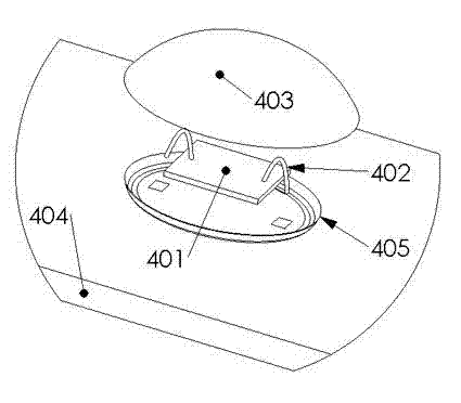
[0066] see figure 1 , which is a LED packaging structure, including: LED chips 401 , inner leads 402 , filling colloid 403 , circuit board 404 , and reflective bowl 405 .

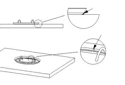
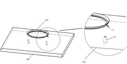
[0067] For a better heat dissipation effect, the circuit board 404 may be made of a material with high thermal conductivity, such as metal or ceramic. The mounting position of the circuit board 404 and the LED chip 401 can also be a plane, a square groove, a rectangular groove, a circular groove, and the like. And in order to fix the LED chip, the circuit board 404 can be connected to the LED chip 401 by dotted with silver glue, gold tin, or insulating heat-conducting glue, or soldering material. In addition, the position of the LED chip 401 can be fixed on the circuit board 404, and a reflective bowl can be added to improve the light extraction efficiency. In order to ensure the shape of the ...


PUM


Abstract

An LED packaging method comprises the following steps of (1) fixing a reflecting bowl / fixing bracket on a circuit board, presetting a plurality of vent holes for a glue filling process, wherein a hollow part at which an LED chip is in direct contact with the circuit board is formed at the bottom of the reflecting bowl / fixing bracket; (2) directly loading and covering the LED chip on the hollow part of the reflecting bowl / fixing bracket, on the circuit board; (3) welding the anode and the cathode of the LED chip on the circuit board by an inner lead wire; and (4) coating a fluorescent powder layer on the surface of the LED chip, filling glue on the LED chip so as to completely cover the LED chip, the inner lead wire and the reflecting bowl / fixing bracket, or filling a mixture of fluorescent powder and glue on the LED chip so as to completely cover the LED chip, the inner lead wire and the reflecting bowl / fixing bracket. According to the method, the advantages of good thermal radiation property, simple structure and good reflecting effect can be achieved.

Description

technical field [0001] The invention relates to a manufacturing process of a lamp, in particular to a manufacturing process of an LED packaging structure and the LED packaging structure. Background technique [0002] LED packaging is to connect the outer leads to the electrodes of the LED chip to facilitate connection with other devices. It not only uses wires to connect the electrodes on the chip to the package shell to complete the connection between the chip and the external circuit, but also fixes and seals the chip to protect the chip circuit from corrosion by water, air and other substances that cause electrical performance degradation. In addition, encapsulation can also improve the light extraction efficiency of LED chips, and facilitate the application, installation and transportation of downstream industries. Therefore, packaging technology plays an important role in the performance and reliability of LEDs. [0003] In the patent No. 200710029336.0, the applicat...

Claims


Application Information

Patent Timeline
IPC IPC(8): H01L33/00H01L33/48H01L33/64
Inventor 陈凯黄建明郭丹傅少钦
Owner ZHEJIANG XIZI OPTOELECTRONICS TECH
Learn More