Electrostatic attenuation time testing device
A decay time, testing device technology, applied in the direction of measuring devices, measuring electricity, measuring electrical variables, etc.
- Summary
- Abstract
- Description
- Claims
- Application Information
AI Technical Summary
Problems solved by technology
Method used
Image
Examples
Embodiment Construction
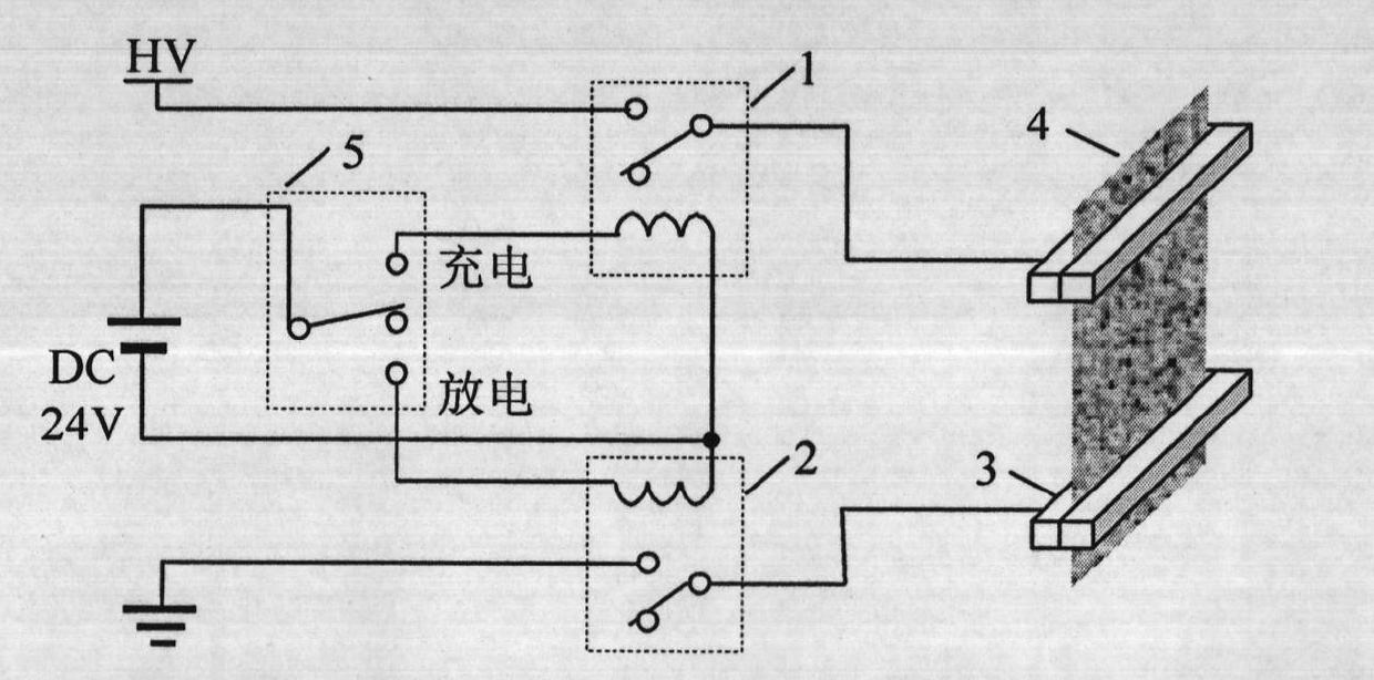
[0016] figure 1 It is the schematic diagram of charge-discharge control circuit when testing samples: 1-vacuum high-voltage switch 1; 2-vacuum high-voltage switch 2; 3-electrode and sample fixture; 4-sample schematic diagram; 5-low voltage control charge-discharge switch.
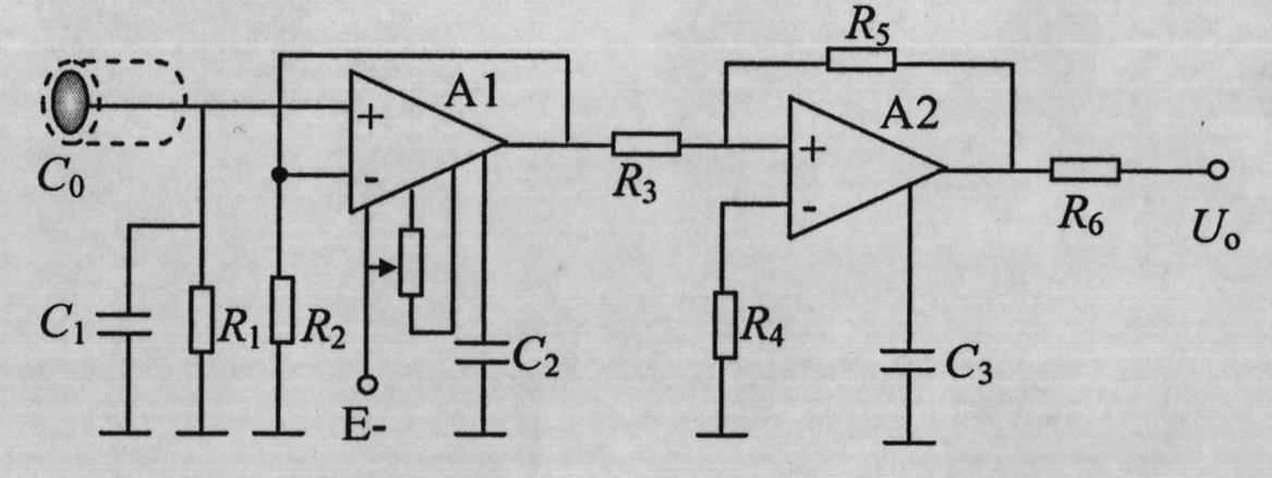
[0017] figure 2 It is a non-contact active sensor electrical schematic diagram: C 0 Indicates the equivalent capacitance of the input probe to the ground; A1 is the emitter follower, A2 is the non-inverting amplifier; R 1 >1GΩ, R 2 >3MΩ, used for zero drift suppression; the circuit is also equipped with zero adjustment and zero reset buttons, which are used to reset the circuit before testing.
[0018] image 3 It is the principle block diagram of the decay time timing device of the present invention: the discharge control signal is used as the trigger signal to make the single chip microcomputer start counting, and the time is displayed by the LED; at the same time, the decay voltage on the sample is ...
PUM
 Abstract
Description
Claims
Application Information


