Semiconductor device forming method

A semiconductor and device technology, which is applied in the field of semiconductor device formation, can solve the problems that nickel silicide cannot be completely removed and affects the conductivity of semiconductor devices, and achieve the effect of improving electrical performance

Active Publication Date: 2014-12-03
SEMICONDUCTOR MANUFACTURING INTERNATIONAL (BEIJING) CORP
View PDF1 Cites 0 Cited by
  • Summary
  • Abstract
  • Description
  • Claims
  • Application Information

AI Technical Summary

Problems solved by technology

[0009] At the same time, if figure 2 As shown, the surface of the sidewall 030 also has part of the silicon dangling bonds, and the silicon dangling bonds will react with the nickel layer 040 to form nickel silicide on the surface of the sidewall 030, and the nickel silicide has The electrical conductivity will make the source / drain region in the substrate electrically connected to the gate 022, which will seriously affect the electrical conductivity of the semiconductor device
[0010] Further, as image 3 As shown, when removing the nickel layer on the surface of the substrate 001 and the surface of the sidewall 030, the nickel silicide on the sidewall 030 cannot be completely removed, resulting in a part of the nickel silicide remaining on the sidewall 030, The nickel silicide has electrical conductivity, which may further cause the source / drain region in the substrate 001 to be electrically connected to the gate 022, seriously affecting the electrical conductivity of the semiconductor device

Method used


Image

  • Semiconductor device forming method
  • Semiconductor device forming method
  • Semiconductor device forming method

Examples


Embodiment Construction

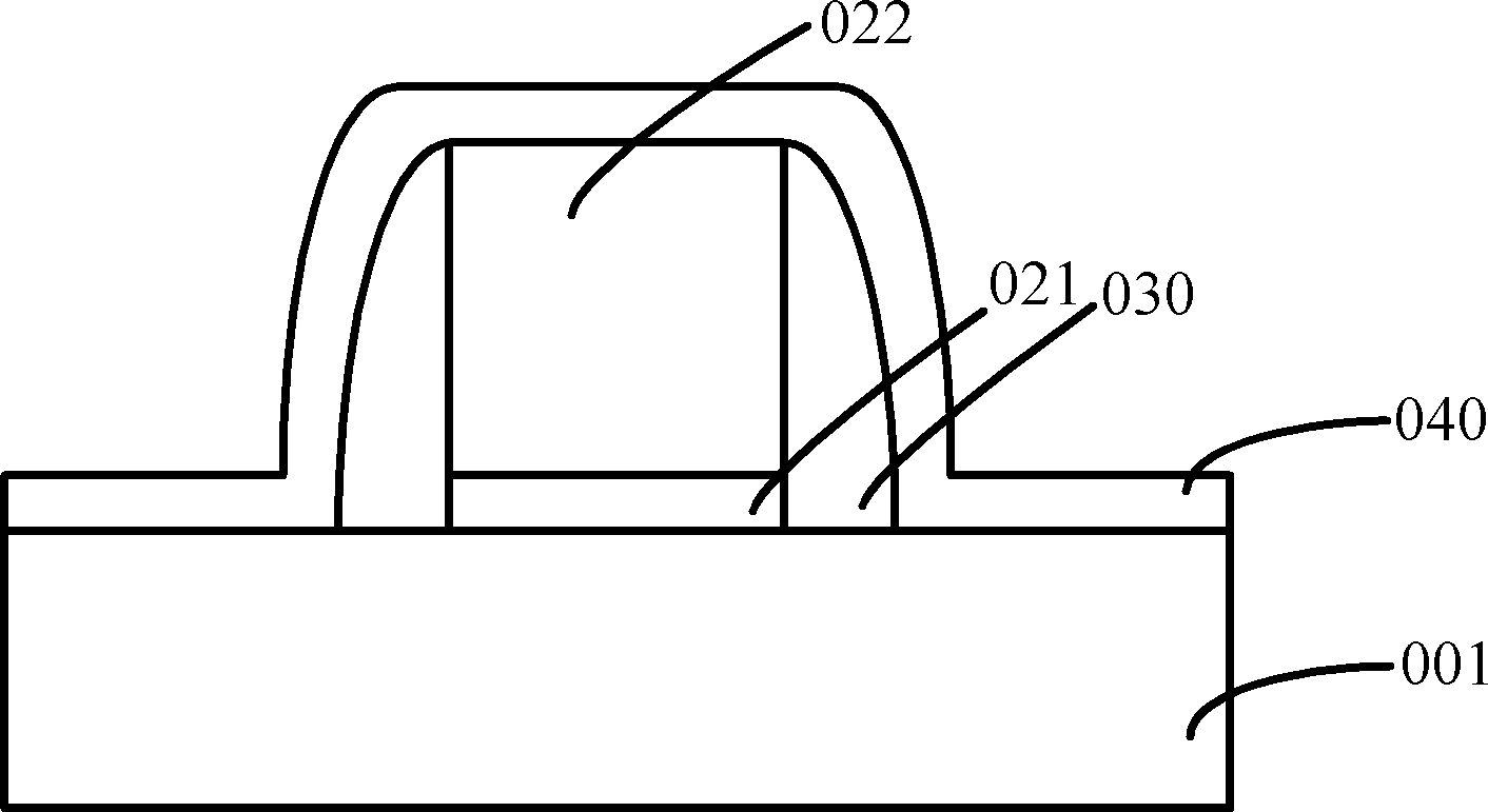
[0035] refer to Figure 1 to Figure 4 , in the process of forming metal silicide in the prior art, because the metal silicide formed by metal diffusion will enhance the leakage phenomenon between the source and drain regions, and the source / drain region and the The gate is electrically connected, which seriously reduces the reliability of the semiconductor's conductive performance.

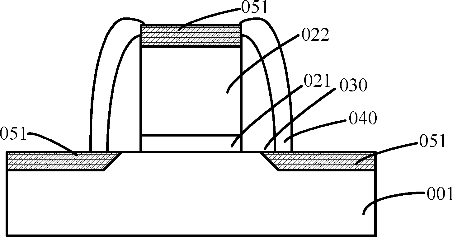
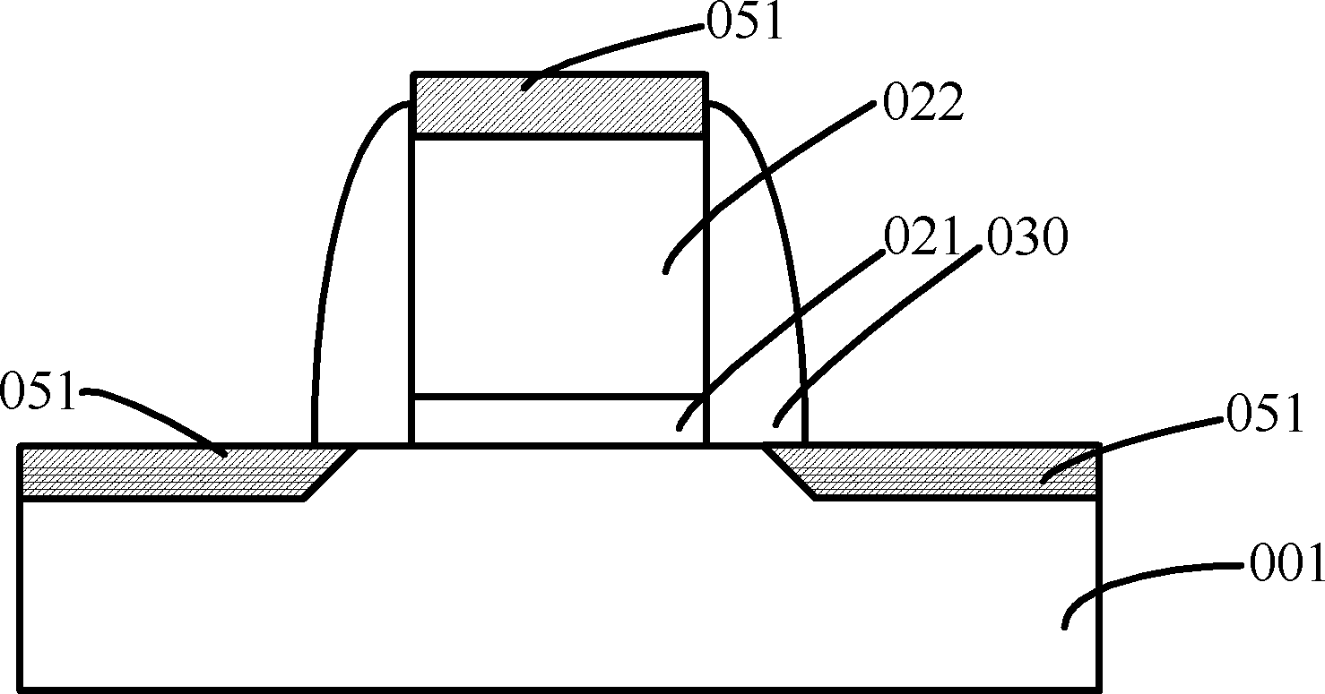
[0036] In order to solve the above problems, the present invention provides a method for forming a semiconductor device, comprising: providing a substrate, a gate structure on the substrate, and sidewalls on both sides of the gate structure; forming an auxiliary spacer on the surface; forming a metal layer on the exposed surface of the substrate and the auxiliary side wall; annealing the metal layer to form a metal silicide in the substrate, and the auxiliary side wall is used to prevent metal The layer is diffused laterally into the sidewalls to avoid the formation of metal silicides on the sidew...


PUM


Abstract

The invention provides a semiconductor device forming method, which comprises the steps that: a substrate, a grid structure positioned on the substrate and side walls positioned at two sides of the grid structure are provided; an auxiliary side wall is formed on the surface of the side walls; a metal layer is formed on the surface of the auxiliary side wall and the exposed substrate; and the metal layer is subjected to annealing, metal silicide is formed in the substrate, the auxiliary side wall is used for preventing the metal layer from transversely diffusing into the side walls, and the formation of the metal silicide on the side walls is avoided. The semiconductor device forming method has the advantages that the auxiliary side wall is formed on the side walls, the gap of the metal silicide in the substrate positioned at two sides of the grid structure is enlarged, the electric leakage performance in an enhancement channel of the metal silicide formed through the metal diffusion is avoided, and the electric connection of a source / drain region and a grid electrode is further avoided, so the performance of a semiconductor device is improved.

Description

technical field [0001] The invention relates to the field of semiconductor manufacturing, in particular to a method for forming a semiconductor device. Background technique [0002] The self-aligned silicide technology is a process technology that reduces the resistance of the gate electrode and the source / drain region by forming a metal silicide layer on the gate electrode and the source / drain region. Nickel silicide layers and cobalt silicide layers are widely used as metal silicide layers. The Chinese patent application with the patent publication number CN101432860A provides a technical solution of using the nickel silicide layer as the metal silicide. [0003] The nickel silicide layer formed by nickel salicide technology may have different composition ratios. For example, the nickel silicide layer can be Ni 2 Si layer, NiSi layer or NiSi 2 any of the layers. Among them, the composition of different silicides is determined by the ratio of nickel to silicon in the r...

Claims


Application Information

Patent Timeline
Patent Type & Authority Patents(China)
IPC IPC(8): H01L21/336H01L21/285H01L21/324
Inventor 李凤莲倪景华
Owner SEMICONDUCTOR MANUFACTURING INTERNATIONAL (BEIJING) CORP
Why Eureka
Try Eureka