Eureka AIR delivers breakthrough ideas for toughest innovation challenges, trusted by R&D personnel around the world.

Detection structure suitable for detecting source and drain conduction and detection method for detection structure

A technology for detecting structure, source and drain, which is used in semiconductor/solid-state device testing/measurement, electrical measurement, measurement device, etc., and can solve problems such as being unsuitable for timely detection and clear observation.

Active Publication Date: 2012-07-11
SEMICON MFG INT (SHANGHAI) CORP +1
View PDF4 Cites 3 Cited by
  • Summary
  • Abstract
  • Description
  • Claims
  • Application Information

AI Technical Summary

Problems solved by technology

[0005] In view of this, the main purpose of the present invention is to provide a detection method using voltage contrast, which is suitable for the detection of source-drain conduction. The detection structure and its detection method

Method used


Image

  • Detection structure suitable for detecting source and drain conduction and detection method for detection structure
  • Detection structure suitable for detecting source and drain conduction and detection method for detection structure
  • Detection structure suitable for detecting source and drain conduction and detection method for detection structure

Examples


Embodiment 1

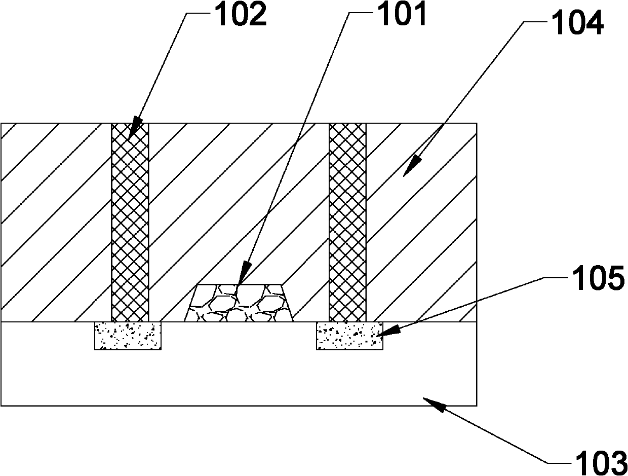
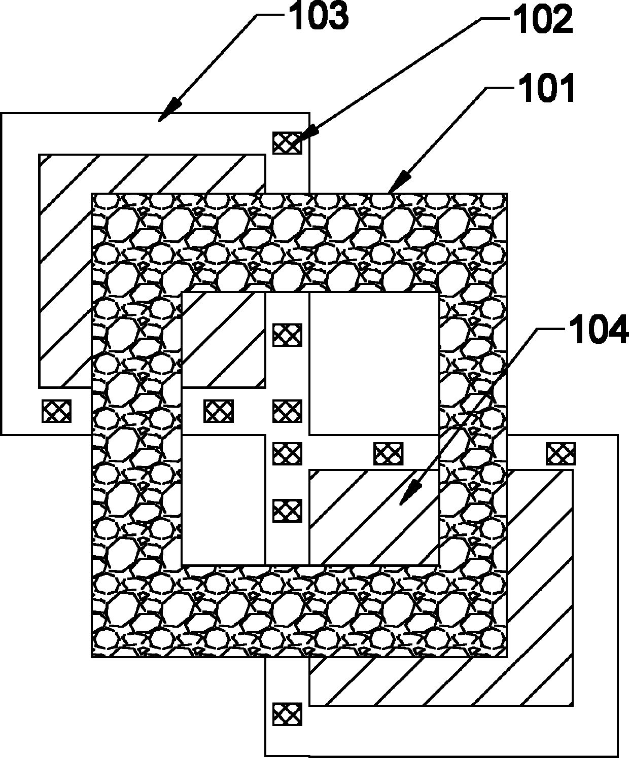
[0025] figure 1 and figure 2 A specific embodiment of the detection structure suitable for source-drain conduction detection of the present invention is shown. Such as figure 1 As shown, the detection structure is disposed on the substrate. Two active area rings 103 with a hollow horizontal cross-section are provided on the substrate, and one corner of each of the two active area rings 103 communicates with each other, as figure 1 shown. A polysilicon ring 101 with a hollow rectangular horizontal cross-section is also provided on the substrate, and the polysilicon ring 101 intersects the two active region rings 103 respectively. Thus, four MOS structures are formed on the four sides near the center of the two polysilicon rings 103 .

[0026] An epitaxial metal 102 is provided at symmetrical positions on both sides of each side of the polysilicon ring 101, and there are more epitaxial metals 102 located in the hollow part of the polysilicon ring 101, a total of 6 are prov...


PUM


Abstract

The invention provides a detection structure suitable for detecting source and drain conduction. The detection structure is arranged on a substrate, and comprises at least one polygonal active area ring of which horizontal section is hollow; at least one polycrystalline silicon grid is arranged on each active area ring; and the polycrystalline silicon grid and the active area rings on two sides of the polycrystalline silicon grid form a metal oxide semiconductor (MOS) structure. The detection structure is suitable for detecting the voltage contrast of epitaxial metals by using an E-beam detection method; and by observing the brightness degree, whether source and drain conduction exists in the detection structure can be clearly displayed, and whether source and drain conduction exists on a wafer can be further judged. Because the problem is early discovered, unnecessary subsequent processing for waste products can be avoided.

Description

technical field [0001] The invention relates to the technical field of integrated circuits, in particular to a detection structure suitable for source-drain conduction detection and a detection method thereof. Background technique [0002] In actual crystals, due to the influence of crystal formation conditions, thermal motion of atoms and other conditions, the arrangement of atoms cannot be so complete and regular, and there are often regions that deviate from the ideal crystal structure. These deviations from the perfectly periodic lattice structure are defects in the crystal, which break the symmetry of the crystal. Crystal defects (Crystal Defects) include plane defects, line defects and point defects, all of which have extremely important effects on the physical properties of crystals. [0003] In the manufacture of integrated circuits, crystal defects can easily lead to leakage conduction between the source and drain of the CMOS in the finished integrated circuit. It...

Claims


Application Information

Patent Timeline
Patent Type & Authority Applications(China)
IPC IPC(8): H01L21/66G01R31/02
Inventor 吴浩李鹤鸣李彬王璐
Owner SEMICON MFG INT (SHANGHAI) CORP
Why Eureka
Eureka Blog
Learn More