Method for increasing maintaining voltage of electrostatic protective device
A technology for maintaining voltage and electrostatic protection, which is applied in the field of increasing the maintaining voltage of electrostatic protection devices, and can solve problems such as difficulty in increasing the maintaining voltage
- Summary
- Abstract
- Description
- Claims
- Application Information
AI Technical Summary
Problems solved by technology
Method used
Image

Examples
preparation example Construction
[0024] When the thyristor with parasitic PNPN, PNPNP or NPNPN structure prepared by the preparation process provided by the present invention is applied in the field of electrostatic protection, the minimum voltage required to maintain the device working in the hysteresis region is improved through this process, reducing The risk of device latch-up is reduced and device reliability is improved.
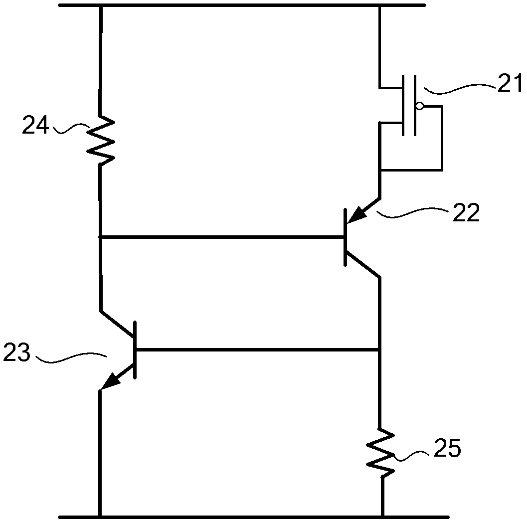
[0025] A method for increasing the maintenance voltage of an electrostatic protection device provided by the present invention is to manufacture thyristor devices with parasitic PNPN, PNPNP, and NPNPN structures on a semiconductor substrate, and to embed such as diodes and diodes in the feedback path of the parasitic transistors of the thyristor devices. Semiconductor components such as strings, transistors or MOS tubes that can suppress the positive feedback of the thyristor, suppress the positive feedback of the thyristor itself, and increase the maintenance voltage of the thyristor ...
Embodiment 1
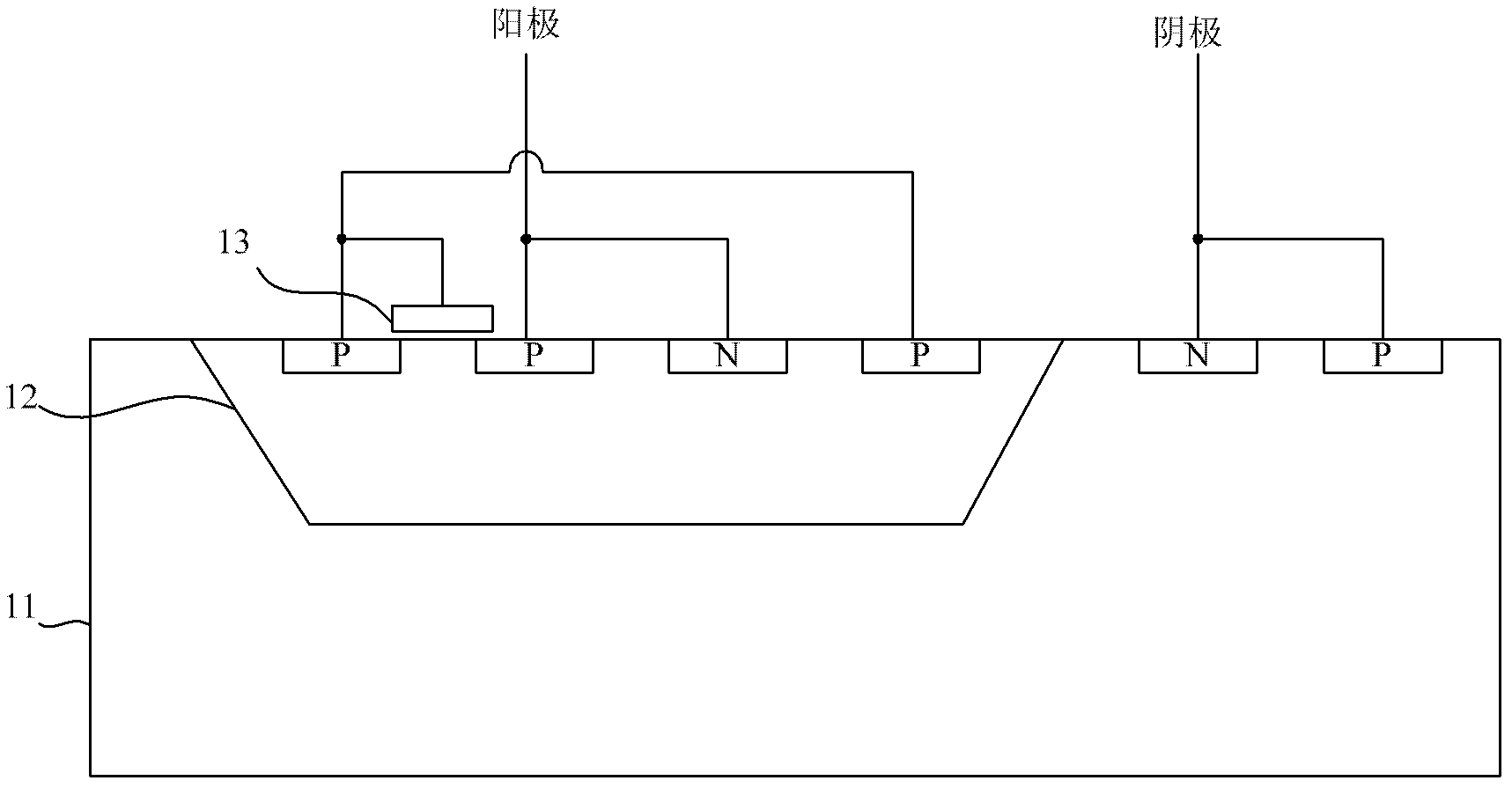
[0029] Such as figure 1 As shown, a kind of method that the present invention provides to improve the maintenance voltage of electrostatic protection device, at first forms the thyristor device of PNPN structure on the semiconductor substrate, embeds MOS tube device on the positive feedback path of parasitic PNP and NPN transistor, suppresses The positive feedback between the parasitic PNP and NPN transistors increases the holding voltage of the thyristor device as an electrostatic protection device. For example, an N well 12 of appropriate concentration is formed on a P-type semiconductor substrate or epitaxy 11 of bulk silicon, and P-type or N-type impurities are implanted to form a high-concentration P+ region or a high-concentration N+ region, which is connected to the anode and cathode as shown in the figure. A parasitic structure of PNPN is formed between them. An embedded PMOS transistor is formed by self-alignment of the polycrystalline gate 13, and a parasitic MOS hi...
Embodiment 2
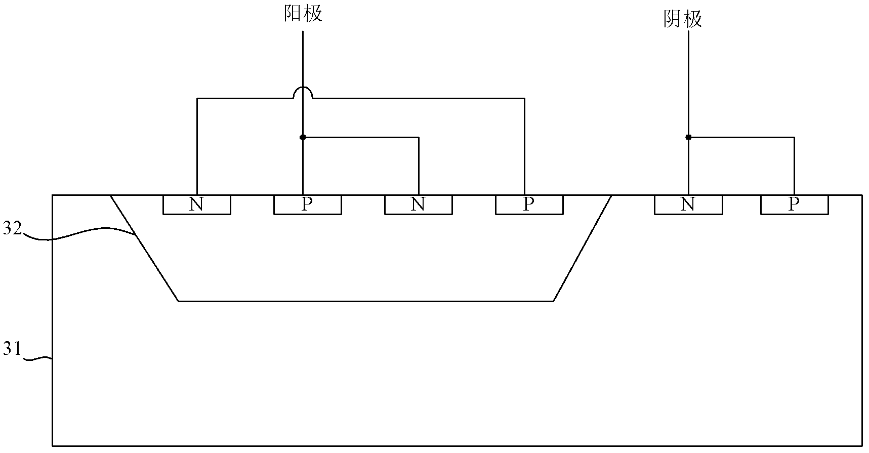
[0032] Such as image 3 As shown, a method for improving the maintenance voltage of an electrostatic protection device provided by the present invention includes first forming a thyristor device with a PNPN structure on a semiconductor substrate, and embedding a diode or a diode string on the positive feedback path of the parasitic PNP and NPN transistors, Suppress the positive feedback between parasitic PNP and NPN transistors, and increase the maintenance voltage of the thyristor device as an electrostatic protection device. For example, an N well 12 of appropriate concentration is formed on a P-type semiconductor substrate or epitaxy 11 of bulk silicon, and P-type or N-type impurities are implanted to form a high-concentration P+ region or a high-concentration N+ region, which is connected between the anode and the N+ region as shown in the figure. A parasitic structure of PNPN is formed between the cathodes. As shown in the figure, a high sustaining voltage silicon contro...
PUM
 Abstract
Description
Claims
Application Information
 - R&D
- Intellectual Property
- Life Sciences
- Materials
- Tech Scout
- Unparalleled Data Quality
- Higher Quality Content
- 60% Fewer Hallucinations
Browse by: Latest US Patents, China's latest patents, Technical Efficacy Thesaurus, Application Domain, Technology Topic, Popular Technical Reports.
© 2025 PatSnap. All rights reserved.Legal|Privacy policy|Modern Slavery Act Transparency Statement|Sitemap|About US| Contact US: help@patsnap.com