Photoelectric chip assembly and packaging method
A photoelectric chip and packaging method technology, applied in the electronic field, can solve the problems of high packaging cost, photoelectric chip corrosion and high temperature damage, large chip size, etc., and achieve the effects of simplifying operation, avoiding corrosion and high temperature damage, and simplifying the packaging process
- Summary
- Abstract
- Description
- Claims
- Application Information
AI Technical Summary
Problems solved by technology
Method used
Image
Examples
Embodiment 1
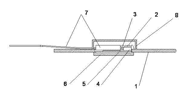
[0028] This embodiment provides an optoelectronic chip assembly, see figure 1 As shown, the figure shows the overall packaging effect of the optoelectronic chip assembly.
[0029] The optoelectronic chip assembly in this embodiment includes: a circuit board 1 with a cavity, a bottom plate 6 located below the cavity and fixed on the bottom of the circuit board 1, an optical fiber fixed on the bottom plate 6 through a first carrier 5 Component 7, the first optoelectronic chip 3 fixed on the base plate 6 through the second carrier 4, and the circuit board 1 with a cavity and the base plate 6 located above the first optoelectronic chip 3 and the optical fiber assembly 7 The cover of the closed space 8.
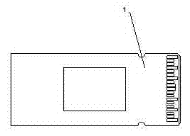
[0030] Wherein, the shape of circuit board 1 refers to figure 2 and image 3 as shown, figure 2 A top view of the circuit board 1 in the optoelectronic chip assembly is given, image 3 A side view of the circuit board 1 in the optoelectronic chip module is given. The circu...
Embodiment 2
[0039] The embodiment of the present invention provides a packaging method for optoelectronic chip components, such as Figure 6 shown, including the following steps:
[0040] S501: Fix the first optoelectronic chip and the optical fiber assembly on the circuit board, and electrically connect the first optoelectronic chip to the circuit board, wherein the light receiving surface of the first optoelectronic chip is connected to the optical fiber assembly The luminous surface is opposite;
[0041] S502: Fix the cover on the circuit board, wherein the cover is located above the optoelectronic chip and the optical fiber assembly, and forms a closed space with the circuit board.
[0042] Preferably, the step of fixing the first optoelectronic chip and the optical fiber assembly on the circuit board specifically includes: affixing and fixing the first carrier on the circuit board, and fixing the optical fiber assembly on the first carrier affixing and fixing the second carrier on ...
PUM
 Abstract
Description
Claims
Application Information


