Transparent electrode material and preparation method thereof
A technology of transparent electrodes and conductive layers, applied in circuits, photovoltaic power generation, electrical components, etc., can solve problems such as instability of flexible substrates, and achieve the effect of easy industrial production, wide application, and industrial production.
- Summary
- Abstract
- Description
- Claims
- Application Information
AI Technical Summary
Problems solved by technology
Method used
Image

Examples
preparation example 1
[0039] Preparation of graphene oxide sol
[0040] To the concentrated sulfuric acid of 98% by weight, the concentration of 1500g is to add 5.0g of natural flaky graphite (particle diameter is 200 μm), 5.0g of sodium nitrate and 25.0g of potassium permanganate, and the resulting mixture is placed in an ice bath at 0°C. After stirring for 5 h under the same conditions (that is, the temperature of the mixture was kept at 0° C. by ice bath), then stirred at 30° C. for 10 h; The concentration of 6mL is the hydrogen peroxide of 30% by weight, after stirring for 1h, filter, then the obtained filter cake is centrifugally washed with hydrochloric acid of 10% by weight, then centrifugally washed with deionized water, and the colloidal product after washing is added to 40 mL of deionized water was ultrasonically dispersed at a power of 200 W to obtain a graphene oxide sol (the content of graphene oxide was 20% by weight, and the content of water was 80% by weight).
Embodiment 1
[0042] This example is to illustrate the preparation method of the b-type transparent electrode material of the present invention.
[0043] (1) Preparation of porous anodized aluminum template: provided by a two-step anodic oxidation method (according to HidekiMasuda and Kenji Fukuda, Ordered Metal Nanohole Arrays Made by a Two-StepReplication of Honeycomb structures of Anodic Alumina, SCIENCE, 268 (9) 1995) method) to prepare a porous anodized aluminum sheet, the aperture of the porous anodized aluminum sheet measured by a scanning electron microscope is 50nm, and the hole spacing is 150nm;
[0044] (2) electron beam evaporation metal layer: use electron beam evaporator (Edwars, AUTO 500) to the anodic aluminum oxide sheet that step (1) obtains and evaporate one deck metal silver, thickness 3nm;
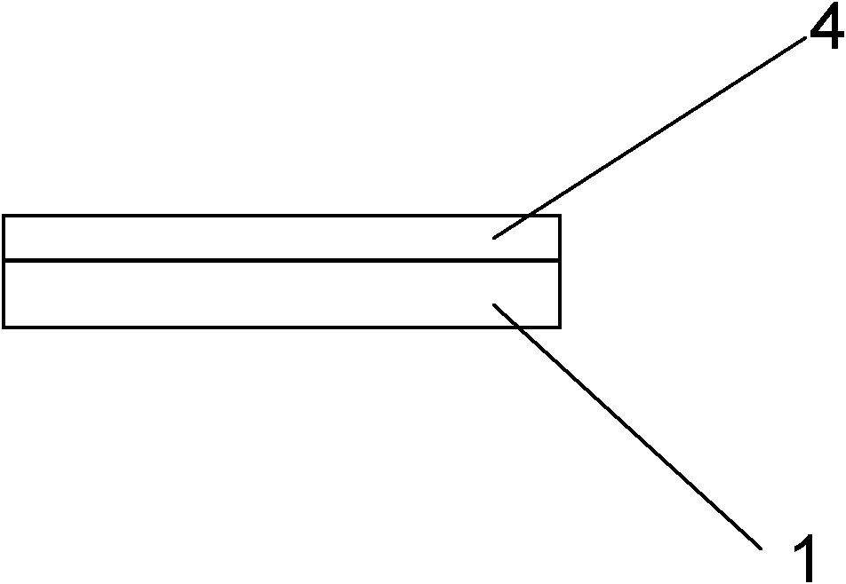
[0045] (3) Remove the alumina template: Place a quartz sheet (Jinzhou Huamei Quartz Electric Appliance Factory, 2cm×2cm in size, 1mm in thickness) under the anodized aluminum sheet ...
Embodiment 2
[0051] This example is to illustrate the preparation method of the b-type transparent electrode material of the present invention.
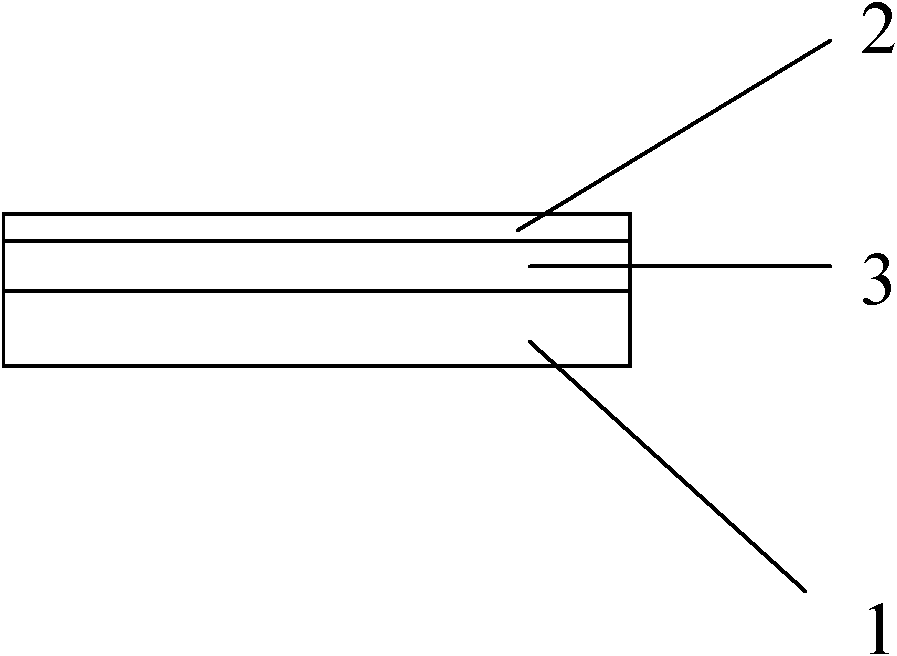
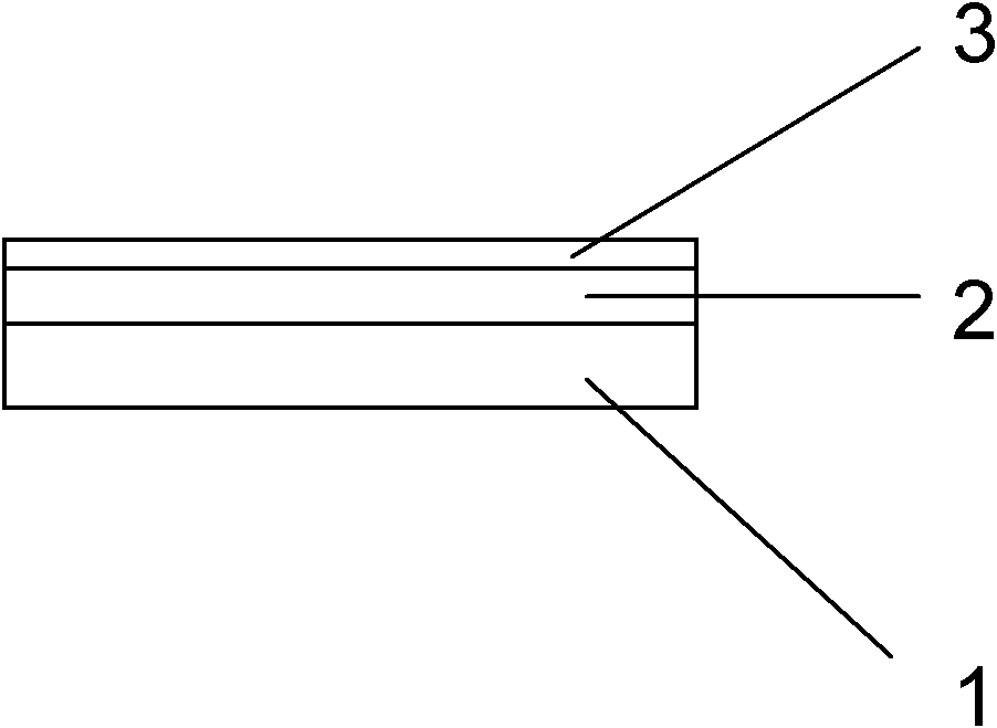
[0052] (1) The method for chemical vapor deposition prepares nitrogen-doped graphene: with coating machine (KYUY Zhongkekeyi Technology Development Co., Ltd., model SBC-2), with Ni as the target material, deposition time 20s, on a quartz sheet ( Jinzhou Huamei Quartz Electric Appliance Factory, with a size of 2cm×2cm and a thickness of 1mm) was thermally evaporated with 50nm thick Ni. Put the quartz piece into the quartz tube, pass hydrogen (20sccm) and argon (100sccm), when the temperature of the center of the furnace rises to 800°C, feed 60sccm of CH4 and 60sccm of NH3, put the quartz tube into the furnace After 10 min, the sample was cooled to room temperature under hydrogen flow to obtain a nitrogen-doped graphene film. The Ni on the film was dissolved with a phosphoric acid solution with a concentration of 1%, and the graphene surface was wa...
PUM
| Property | Measurement | Unit |
|---|---|---|
| Sheet resistance | aaaaa | aaaaa |
| Thickness | aaaaa | aaaaa |
| Thickness | aaaaa | aaaaa |
Abstract
Description
Claims
Application Information
 - R&D Engineer
- R&D Manager
- IP Professional
- Industry Leading Data Capabilities
- Powerful AI technology
- Patent DNA Extraction
Browse by: Latest US Patents, China's latest patents, Technical Efficacy Thesaurus, Application Domain, Technology Topic.
© 2024 PatSnap. All rights reserved.Legal|Privacy policy|Modern Slavery Act Transparency Statement|Sitemap