Vacuum package structure and vacuum packaging method for wafer-level MEMS (micro-electromechanical system) devices
A vacuum packaging and wafer-level technology, applied in the direction of microstructure devices, manufacturing microstructure devices, microstructure technology, etc., can solve the development trend that is not conducive to the miniaturization of MEMS devices, the reduction of integration degree, and the increase of packaging area. Problems such as , to achieve compact structure, improve production efficiency, and improve the effect of integration
- Summary
- Abstract
- Description
- Claims
- Application Information
AI Technical Summary
Problems solved by technology
Method used
Image

Examples
Embodiment 1
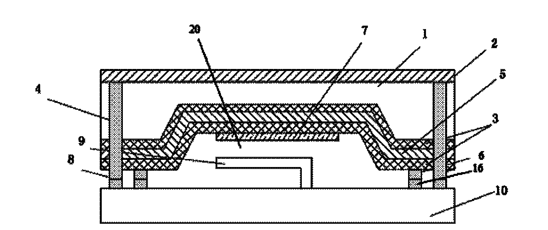
[0072] like figure 1 As shown: the embodiment of the present invention adopts the 3D packaging technology of TSV (Through Silicon Vias) to realize the connection form of the ASIC circuit 2 and the MEMS structure 9 . Specifically, a TSV conductive via 4 is provided in the first wafer 1, the upper end of the TSV conductive via 4 is electrically connected to the ASIC circuit 2, and the lower end of the TSV conductive via 4 is electrically connected to the second conductive bump 15. , the second conductive bump 15 is located outside the first bonding ring 6 . First conductive bumps 8 are provided on the second wafer 10 , the second conductive bumps 8 are electrically connected to the MEMS structure 9 , and the first conductive bumps 8 are located directly below the second conductive bumps 15 . When the first bonding ring 6 and the second bonding ring 16 form the vacuum cavity 20 through vacuum bonding, the first conductive bump 8 is electrically connected to the second conductive...
Embodiment 2
[0097] like Figure 11 and Figure 20 As shown: the second wafer 10 is provided with a first conductive electrode 11, and the first conductive electrode 11 is located outside the MEMS structure 9; The two conductive electrodes 19 are electrically connected to form an electrical connection path between the MEMS structure 9 and the ASIC circuit 2 . The materials of the first conductive electrode 11 and the second conductive electrode 19 are generally selected from conventional semiconductor electrode materials such as gold and the like. After the second conductive electrode 19 is formed on the ASIC circuit 2, and the first conductive electrode 11 is formed on the second wafer 10, the first conductive electrode 11 and the second conductive electrode 11 are connected to the second conductive electrode 12 through the bonding wire 12 by the wire bonding equipment. 12 electrical connections.
[0098] like Figure 12~Figure 20 Shown: the wafer-level MEMS device vacuum structure of...
PUM
 Abstract
Description
Claims
Application Information
 - Generate Ideas
- Intellectual Property
- Life Sciences
- Materials
- Tech Scout
- Unparalleled Data Quality
- Higher Quality Content
- 60% Fewer Hallucinations
Browse by: Latest US Patents, China's latest patents, Technical Efficacy Thesaurus, Application Domain, Technology Topic, Popular Technical Reports.
© 2025 PatSnap. All rights reserved.Legal|Privacy policy|Modern Slavery Act Transparency Statement|Sitemap|About US| Contact US: help@patsnap.com