Sun-shading type double-silver low-radiation coated glass capable being tempered
A low-radiation coating and glass technology, which is applied in the coating field of glass deep processing, can solve the problems of inability to meet high-performance product requirements, poor oxidation resistance, and product yield decline, and achieve strong oxidation resistance and strong adhesion , The effect of small data drift
- Summary
- Abstract
- Description
- Claims
- Application Information
AI Technical Summary
Problems solved by technology
Method used
Image
Examples
specific Embodiment 1
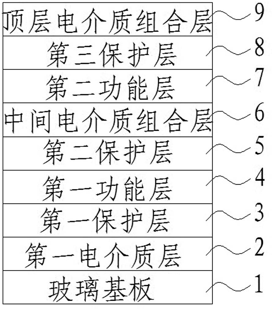
[0053] The specific material structure of the film in this embodiment is:
[0054] Glass substrate / Si 3 N 4 / NiCr / Ag / NiCr / ZnSnO 3 / ZnO / Ag / NiCr / ZnSnO 3 / Si 3 N 4 .
[0055] In the above structure:
[0056] The first Si of the first dielectric layer 2 3 N 4 The film thickness of the layer is 21.1nm;
[0057] The thickness of the NiCr layer of the first protective layer 3 is 0.9 nm;
[0058] The thickness of the Ag layer of the first functional layer 4 is 14.3 nm;
[0059] The thickness of the NiCr layer of the second protective layer 5 is 2.1 nm;
[0060] The first ZnSnO of the intermediate dielectric combination layer 6 3 The layer thickness is 63nm;
[0061] The thickness of the 6-layer ZnO layer of the middle dielectric composite layer is 10nm;
[0062] The thickness of the Ag layer of the second functional layer 7 is 15.6 nm;
[0063] The thickness of the NiCr layer of the third protective layer 8 is 0.6 nm;
[0064] The second ZnSnO of the top dielectric combination layer 9 3 The layer thi...
specific Embodiment 2
[0071] The specific material structure of the film in this embodiment is:
[0072] Glass substrate / Si 3 N 4 / NiCr / Ag / NiCr / ZnSnO 3 / ZnO / Ag / NiCrOx / ZnSnO 3 / Si 3 N 4 .
[0073] In the above structure:
[0074] The first Si of the first dielectric layer 2 3 N 4 The film thickness of the layer is 34.8nm;
[0075] The thickness of the NiCr layer of the first protective layer 3 is 2.7 nm;
[0076] The thickness of the Ag layer of the first functional layer 4 is 9.5 nm;
[0077] The thickness of the NiCr layer of the second protective layer 5 is 2.7 nm;
[0078] The first ZnSnO of the intermediate dielectric combination layer 6 3 The layer thickness is 84.1nm;
[0079] The thickness of the ZnO layer of the intermediate dielectric composite layer 6 is 5.0 nm;
[0080] The thickness of the Ag layer of the second functional layer 7 is 15.9 nm;
[0081] The thickness of the NiCrOx layer of the third protective layer 8 is 1.9 nm;
[0082] The second ZnSnO of the top dielectric combination layer 9 3 The la...
specific Embodiment 3
[0092] The specific material structure of the film in this embodiment is:
[0093] Glass substrate / Si 3 N 4 / NiCrOx / Ag / NiCrOx / ZnSnO 3 / ZnO / Ag / NiCrOx / ZnSnO 3 / Si 3 N 4 .
[0094] In the above structure:
[0095] The first Si of the first dielectric layer 2 3 N 4 The thickness of the layer is 36.7nm;
[0096] The thickness of the NiCr layer of the first protective layer 3 is 3.0 nm;
[0097] The thickness of the Ag layer of the first functional layer 4 is 10.9 nm;
[0098] The thickness of the NiCr layer of the second protective layer 5 is 3.0 nm;
[0099] The first ZnSnO of the intermediate dielectric combination layer 6 3 The layer thickness is 84.7nm;
[0100] The thickness of the 6-layer ZnO layer of the intermediate dielectric composite layer is 5.0 nm;
[0101] The thickness of the Ag layer of the second functional layer 7 is 17.0 nm;
[0102] The thickness of the NiCrOx layer of the third protective layer 8 is 2.4 nm;
[0103] The second ZnSnO of the top dielectric composite layer 8 3 Th...
PUM
| Property | Measurement | Unit |
|---|---|---|
| Film thickness | aaaaa | aaaaa |
| Thickness | aaaaa | aaaaa |
| Thickness | aaaaa | aaaaa |
Abstract
Description
Claims
Application Information


