Circuit and method for testing reliability of integrated circuit

A technology of integrated circuits and test circuits, applied in the field of integrated circuit reliability test circuits and testing

Active Publication Date: 2012-07-18
FUDAN UNIV
View PDF4 Cites 19 Cited by
  • Summary
  • Abstract
  • Description
  • Claims
  • Application Information

AI Technical Summary

Problems solved by technology

Also, HCI degradation cannot be ignored

Method used


Image

  • Circuit and method for testing reliability of integrated circuit
  • Circuit and method for testing reliability of integrated circuit
  • Circuit and method for testing reliability of integrated circuit

Examples


Embodiment Construction

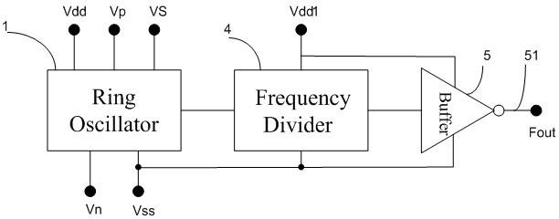
[0026] The circuit and method of the invention are used for testing the reliability of integrated circuits, especially for NBTI degradation testing of pMOSFETs in integrated circuits, PBTI degradation testing of nMOSFETs, and HCI degradation testing of pMOSFETs and nMOSFETs. The whole circuit as figure 1 As shown, there are a total of 7 external electrical contact pads (Pad), which are the high power supply terminal Vdd of the core circuit, the high power supply terminal Vdd1 of the frequency divider and buffer, and the common low power supply terminal of the core circuit, frequency divider and buffer Vss, three control terminals VS, Vp and Vn, the output terminal Fout of the circuit.

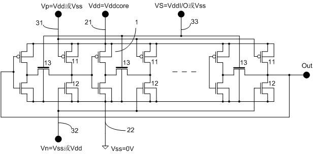
[0027] figure 2 It is the core circuit composed of ring oscillator RO, switch S and auxiliary nMOSFETs and pMOSFETs. The core circuit includes a ring oscillator RO (1). Between each two-stage inverter of RO, a group of auxiliary pMOSFETs (11) and nMOSFETs (12) are connected, and the sources...


PUM


Abstract

The invention belongs to the technical field of integrated circuit test, and in particular relates to a circuit and a method for testing reliability of an integrated circuit. According to the core circuit of the testing circuit, auxiliary p-type metal oxide semiconductor field effect transistors (pMOSFETs) and n-type metal oxide semiconductor field effect transistors (nMOSFETs) are connected between every two stages of inverters of a ring oscillator (RO) and between a high level Vdd and low potential Vss, and a switch transistor is plugged in an input and output connecting line. By controlling the grid voltages of the auxiliary transistors and the switch transistor, normal oscillation of the RO can be realized in the core circuit, dynamic stress is applied to complementary metal oxide semiconductor field effect transistors (CMOSFETs) of the RO, and negative bias temperature instability (NBTI), positive bias temperature instability (PBTI) and hot carrier injection (HCI) stresses are respectively applied to the pMOSFETs or the nMOSFETs of the RO. The testing circuit has the functions of: degradation measurement of the pMOSFETs in the RO under the NBTI stress, degradation measurement of the nMOSFETs under the PBTI stress, degradation measurement of the pMOSFETs under the HCI stress, degradation measurement of the nMOSFETs under the HCI stress, and comparison with degradation measurement of the CMOSFETs under the dynamic stress.

Description

technical field [0001] The invention belongs to the technical field of integrated circuit testing, in particular to an integrated circuit reliability testing circuit and method, in particular to pMOSFETs in integrated circuits under negative bias temperature instability (NBTI) stress, and nMOSFETs in positive bias temperature instability Degradation tests of pMOSFETs and nMOSFETs under hot carrier injection (HCI) stress under PBTI stress, respectively. Background technique [0002] Complementary metal oxide semiconductor field effect transistors are recorded as CMOSFETs; the inverter (Inverter) composed of pMOSFET and nMOSFET is the basic device unit of CMOS integrated circuits, and the characteristic degradation of pMOSFET and nMOSFET is one of the basic reasons for limiting the life of integrated circuits , the degradation reasons are negative bias temperature instability (NBTI) of pMOSFET, positive bias temperature instability (PBTI) of nMOSFET, hot hole injection (HHI) ...

Claims


Application Information

Patent Timeline
Patent Type & Authority Applications(China)
IPC IPC(8): G01R31/3181
Inventor 彭嘉黄大鸣李名复
Owner FUDAN UNIV
Why Eureka
Try Eureka