Manufacture method of Zener diode

A Zener diode and manufacturing method technology, applied in semiconductor/solid-state device manufacturing, electrical components, circuits, etc., can solve the problems of reducing device size, increasing packaging cost, and large lateral diffusion area, and achieving reduced area, The effect of avoiding the enlargement of the lateral diffusion area and improving the integration degree

Active Publication Date: 2012-07-18
ADVANCED SEMICON MFG CO LTD
View PDF3 Cites 17 Cited by
  • Summary
  • Abstract
  • Description
  • Claims
  • Application Information

AI Technical Summary

Problems solved by technology

Although this process is simple, it increases the packaging cost and is not conducive to reducing the size of the device.
Another existing technology for integrating Zener diodes and PIN diodes is to grow a high-resistivity N-type epitaxial layer on a highly doped P-type substrate, and diffuse N-type impurities through the N-type epita

Method used


Image

  • Manufacture method of Zener diode
  • Manufacture method of Zener diode
  • Manufacture method of Zener diode

Examples


Embodiment Construction

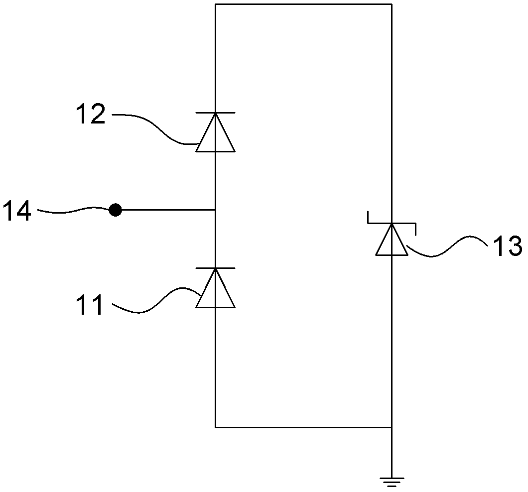
[0032] In order to make the purpose and features of the present invention more obvious and understandable, the specific implementation manners of the present invention will be further described below in conjunction with the accompanying drawings.

[0033] Manufacturing method of the present invention comprises the following steps:

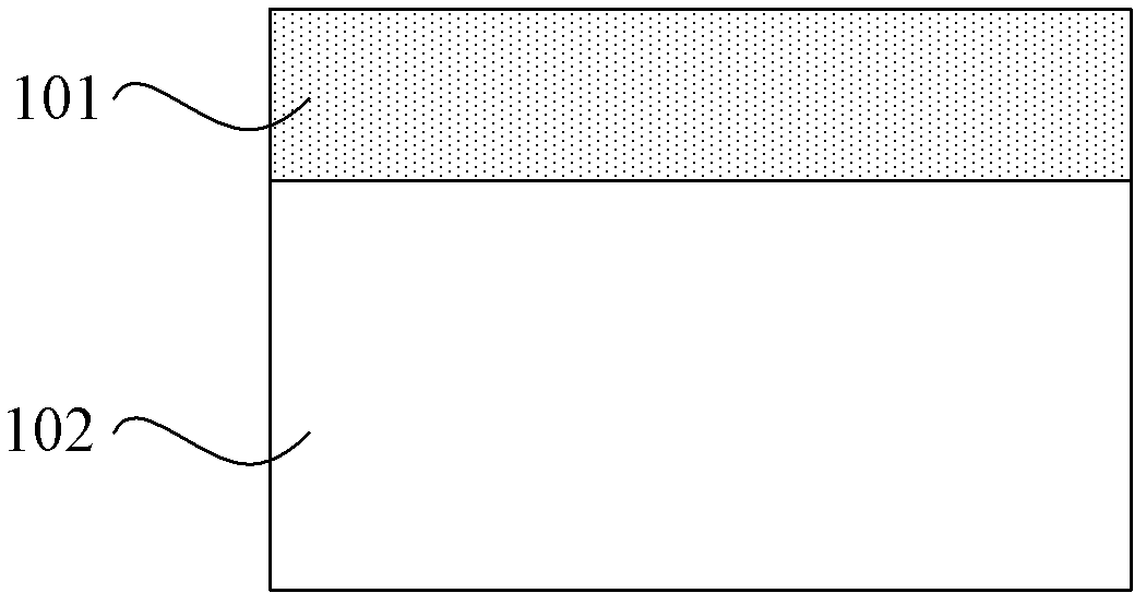
[0034] A substrate is provided, the substrate includes a front surface and a back surface opposite to the front surface, and an epitaxial layer is formed on the front surface of the substrate;

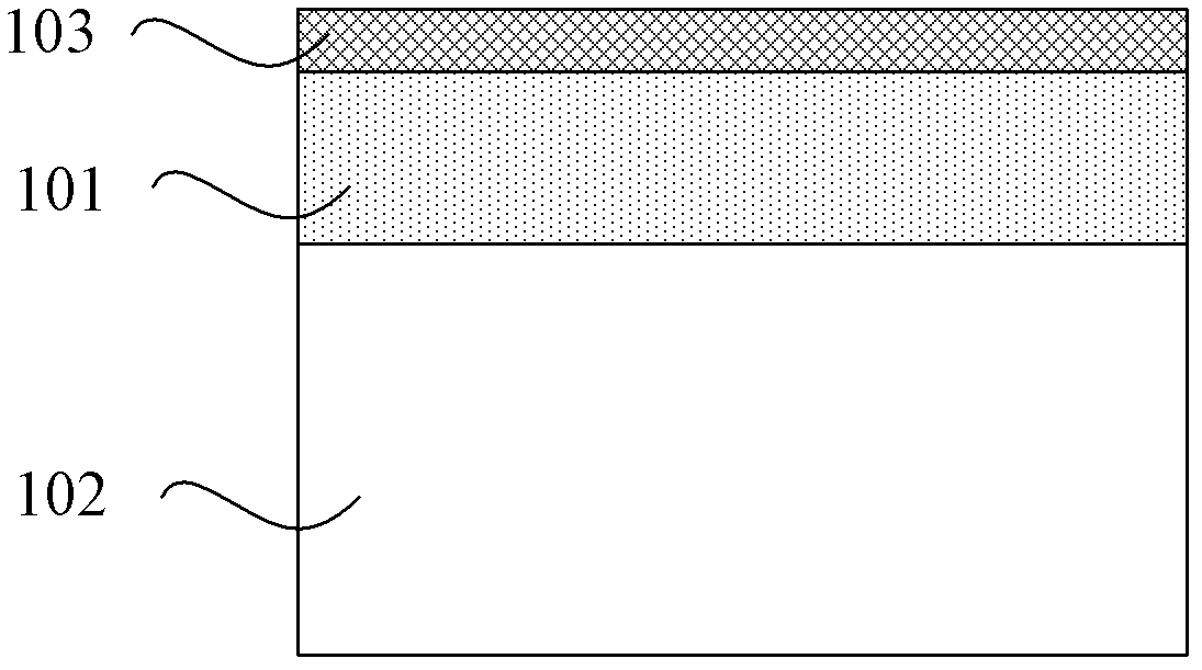
[0035] Etching the epitaxial layer and the partial thickness of the substrate to form a first deep groove, the first deep groove is ring-shaped;

[0036] forming an insulating layer on the epitaxial layer, and simultaneously filling the first deep trench to form a first deep trench filling;

[0037] Etching the insulating layer, the epitaxial layer and the partial thickness of the substrate to form a patterned insulating layer, and forming at least one sec...


PUM

PropertyMeasurementUnit
Thicknessaaaaaaaaaa
Resistivityaaaaaaaaaa
Thicknessaaaaaaaaaa

Abstract

The invention discloses a manufacture method of a Zener diode. The manufacture method comprises the steps of: providing a substrate with an epitaxial layer; etching the epitaxial layer and partial thickness of substrate to form a first annular deep groove; forming an insulation layer on the epitaxial layer while forming a first deep groove filling; etching the epitaxial layer and partial thickness of substrate, forming at least one second deep groove in a region enclosed by the first deep groove; forming in situ doped polycrystalline silicon on the imaged insulation layer while forming a second groove filling; annealing the substrate to form a diffusion region, wherein the diffusion region and the substrate form a PN junction of the Zener diode; etching in situ doped polycrystalline silicon to form the imaged polycrystalline silicon to be used as a cathode of the Zener diode; and forming a metal layer on the back surface of the substrate, wherein the metal layer is used as an anode of the Zener diode. According to the invention, the deep groove process is used for replacing the traditional high-temperature diffusion method, thus the area of a device can be greatly reduced and the integrated level of the integrated circuit is improved.

Description

technical field [0001] The invention relates to the field of integrated circuit manufacturing, in particular to a method for manufacturing Zener diodes. Background technique [0002] Transient interference of voltage and current is the main cause of damage to electronic circuits and equipment, and often brings incalculable losses to people. These disturbances usually come from the start-stop operation of power equipment, the instability of the AC power grid, lightning strike interference, electrostatic discharge and other transient disturbances that are almost everywhere and all the time, making people feel hard to guard against. A transient voltage suppressor (Transient Voltage Suppressor, TVS) is a high-efficiency protection device in the form of a diode. When the two poles of the TVS diode are impacted by reverse transient high energy, it can change the high impedance between its two poles to low impedance at a speed of 10 minus 12 seconds, absorbing surge power up to se...

Claims


Application Information

Patent Timeline
IPC IPC(8): H01L21/329
Inventor 梁博
Owner ADVANCED SEMICON MFG CO LTD
Why Eureka
Try Eureka