Method and device for measuring surface shape error of optical element at high precision

An optical element, surface error technology, applied in the direction of using optical devices, measuring devices, instruments, etc., can solve the problems of high price, complicated interferometer calibration operation, high test environment requirements, low cost, simple test and calibration process. quick effect

Inactive Publication Date: 2014-12-24
CHANGCHUN INST OF OPTICS FINE MECHANICS & PHYSICS CHINESE ACAD OF SCI
View PDF3 Cites 2 Cited by
  • Summary
  • Abstract
  • Description
  • Claims
  • Application Information

AI Technical Summary

Problems solved by technology

[0002] The precise detection of the surface error of optical components usually uses the method of interferometry. It is necessary to calibrate the measurement error of the interferometer when using the interferometer for a long time. The calibration operation of the interferometer is very cumbersome and expensive, and the impact on the test environment very demanding

Method used


Image

  • Method and device for measuring surface shape error of optical element at high precision
  • Method and device for measuring surface shape error of optical element at high precision
  • Method and device for measuring surface shape error of optical element at high precision

Examples


specific Embodiment approach 1

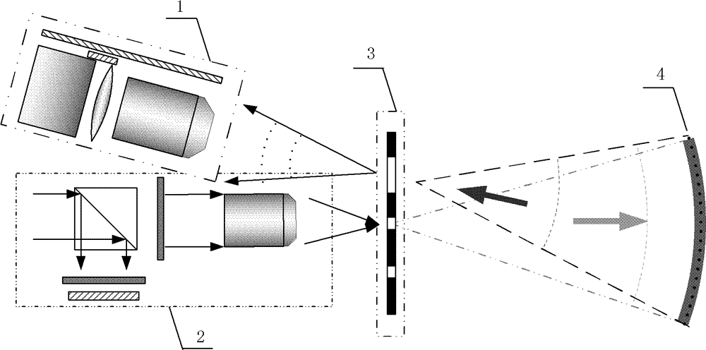
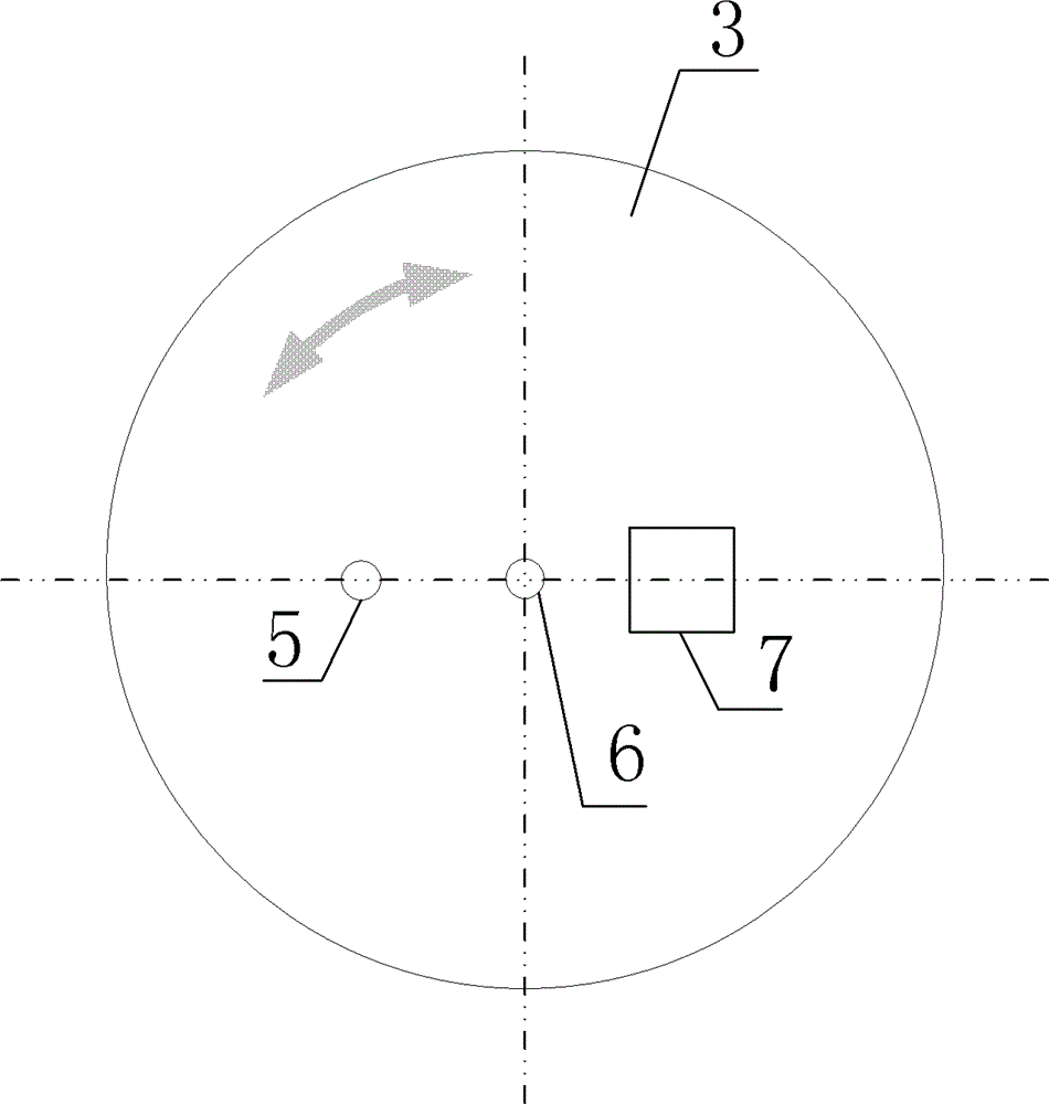
[0016] Specific implementation mode 1. Combination Figure 1 to Figure 4 Describe this embodiment mode, a kind of high-precision testing device of optical element surface shape error described in this embodiment mode, detection device 1, illumination system 2, rotatable small hole plate 3 and optical element 4 to be tested; Small orifice plate 3 is provided with small hole 5, central hole 6 and square hole 7; Rotatable small orifice plate 3 rotates with central hole 6 as the center of circle; The distances of the holes 6 are equal, and the diameters of the central holes 6 are respectively λ / 2NA, wherein NA is the numerical aperture of the optical element to be measured; λ is the wavelength of the light beam emitted by the illumination system 2; the light beam emitted by the illumination system 2 passes through the rotatable The central hole 6 of the small hole plate 3 produces an ideal test beam, which is collected by the detection device 1 after being reflected and converged ...

specific Embodiment approach 2

[0020] Specific embodiment 2. A high-precision testing method for the surface shape of an optical element, the method is realized by the following steps:

[0021] Step A, building a detection platform for the optical imaging system;

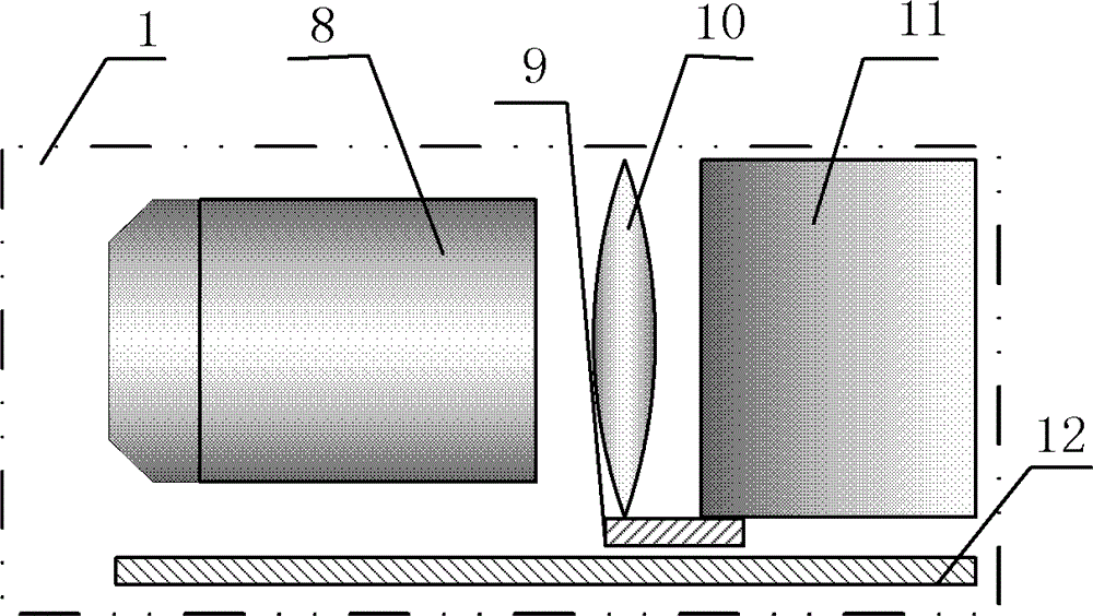
[0022] Step B, align the detection device 1 in the detection platform described in step one with the small hole 5 on the rotatable small hole plate 3, and move the precision axial fine-tuning guide rail 9 in the detection device 1 back and forth to obtain 5 different out-of-focus star point images of diffraction;

[0023] Step C, calculating the optical wavefront error of the detection device 1;

[0024] Step D, align the detection device 1 in the detection platform described in step one with the larger square hole 7 on the rotatable small orifice plate 3, and move the precision axial fine-tuning guide rail 9 in the detection device 1 back and forth, so that Obtain different out-of-focus star point images passing through the square hole 7;

[...


PUM


Abstract

The invention relates to a method and device for measuring the surface shape error of an optical element at high precision, belonging to the technical field of optical testing. The device is low in cost and can be used for measuring rapidly and conveniently at high precision and correcting the measurement error per se and has a relatively low requirement for the measurement environment. According to the method and the device, the principles of the phase recovery method and the point diffraction interferometer are merged together, and a small hole is used for generating ideal spherical waves for the device, thus the surface shape error of the optical element is measured at high precision. The method and the device can be used for measuring the surface shape error of the optical element, and the device can be calibrated at high precision. The method and the device have the characteristics of low cost and high precision and can be used by the optical imaging system producing enterprises and the optical imaging system studying and detecting units.

Description

technical field [0001] The invention relates to the technical field of optical testing, in particular to a high-precision testing method for surface error of optical elements. Background technique [0002] The precise detection of the surface error of optical components usually uses the method of interferometry. It is necessary to calibrate the measurement error of the interferometer when using the interferometer for a long time. The calibration operation of the interferometer is very cumbersome and expensive, and the impact on the test environment The requirements are also very high. The method of phase recovery to detect the surface shape of optical components is being extensively researched. AugustusJ.E.MJanssen extended the Nijboer-Zernike theory and obtained the ExtendedNijboer-Zernike (ENZ) theory, which can be applied to the calculation of the optical point spread function in the case of defocus. JosephJ.M.Braat, Peter Dirksen, AugustusJ.E.MJanssen, ArthurS.vandeNes...

Claims


Application Information

Patent Timeline
Patent Type & Authority Patents(China)
IPC IPC(8): G01B11/24
Inventor 马冬梅邵晶
Owner CHANGCHUN INST OF OPTICS FINE MECHANICS & PHYSICS CHINESE ACAD OF SCI
Why Eureka
Try Eureka