Novel non-refrigeration infrared sensor wafer-level packaging method compatible with CMOS (Complementary Metal Oxide Semiconductor)-MEMS (Micro-Electro-Mechanical System)

A wafer-level packaging and uncooled infrared technology, which is applied in the manufacture of microstructure devices, decorative arts, microstructure devices, etc., can solve the problems of increasing the complexity of processing technology, materials that cannot be used in factories, and environmental protection. Mass production, easy mass production, low cost effect

Inactive Publication Date: 2012-08-15
WUHAN GUIDE INFRARED CO LTD
View PDF7 Cites 10 Cited by
  • Summary
  • Abstract
  • Description
  • Claims
  • Application Information

AI Technical Summary

Problems solved by technology

In addition, the solders used in early wafer-level packaging are gold-tin alloys, lead-tin alloys, etc. These materials cannot be used in factories and are not compatible with standard complementary metal oxide semiconductor (CMOS) processes.
And these materials ar

Method used


Image

  • Novel non-refrigeration infrared sensor wafer-level packaging method compatible with CMOS (Complementary Metal Oxide Semiconductor)-MEMS (Micro-Electro-Mechanical System)
  • Novel non-refrigeration infrared sensor wafer-level packaging method compatible with CMOS (Complementary Metal Oxide Semiconductor)-MEMS (Micro-Electro-Mechanical System)
  • Novel non-refrigeration infrared sensor wafer-level packaging method compatible with CMOS (Complementary Metal Oxide Semiconductor)-MEMS (Micro-Electro-Mechanical System)

Examples


Embodiment Construction

[0018] The present invention will be further described in conjunction with the accompanying drawings.

[0019] The purpose and technical solutions of the present invention will be described in detail below in conjunction with specific examples. The etching process, the film material growth process, and the dry etching process are all existing processes.

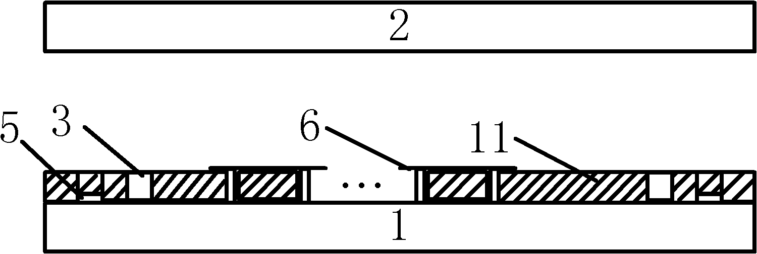
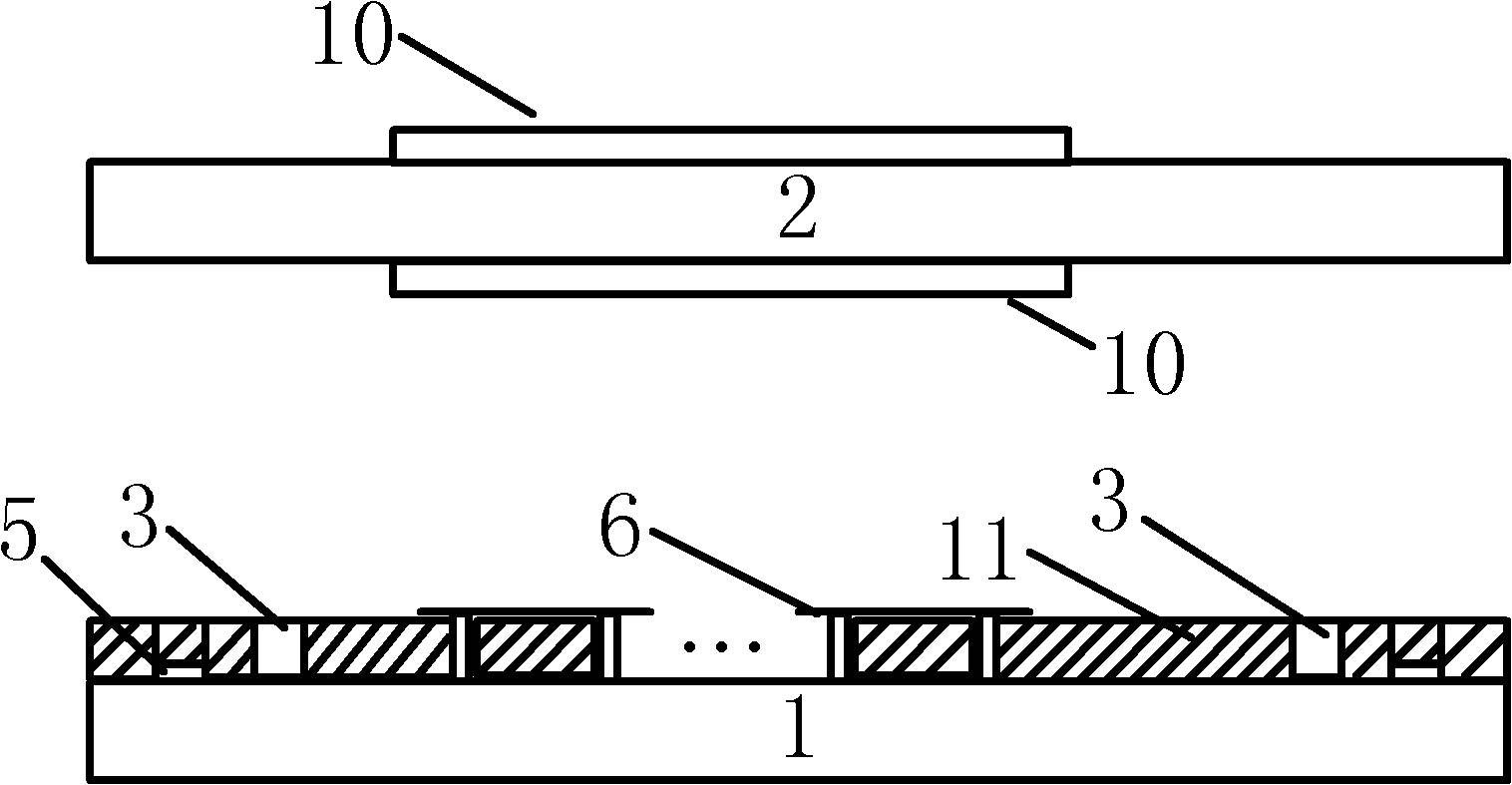
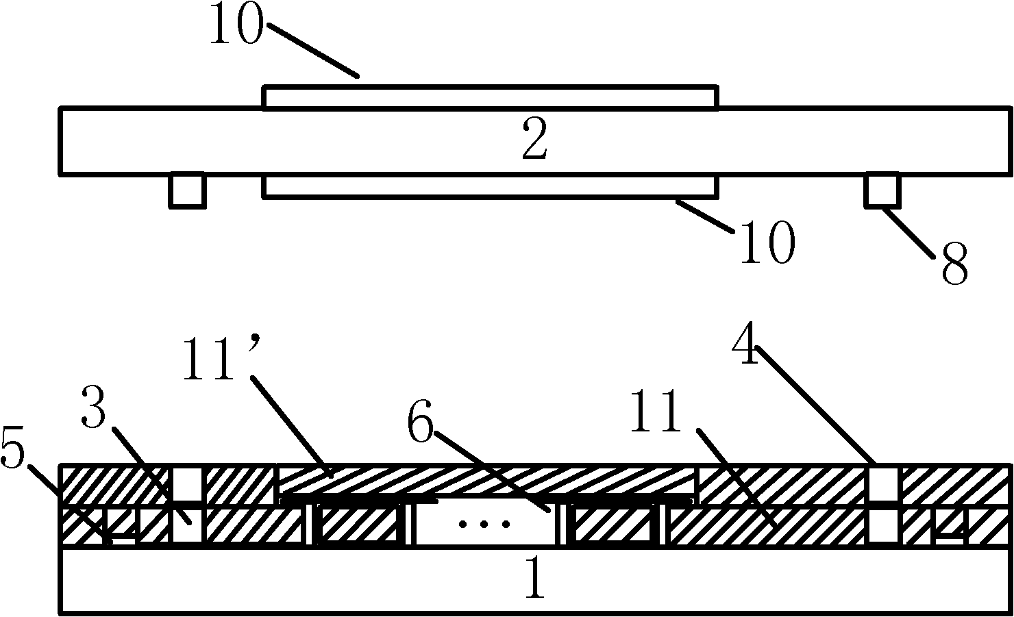
[0020] Such as figure 1 , figure 2 As shown, the device wafer 1 has a readout circuit 5, a detector sensitive element 6, a first sacrificial layer 11 and a first structural layer 3, the thickness of the first sacrificial layer 11 is 2-2.5um, and the first structural layer 3 and the height of the detector sensitive element 6 are consistent with the height of the first sacrificial layer 11, the first sacrificial layer 11 is not released, and the material 3 of the first structural layer is silicon nitride or silicon oxide; image 3 As shown, the second sacrificial layer 11' is prepared on the device wafer 1 with a thickness ...


PUM

PropertyMeasurementUnit
Thicknessaaaaaaaaaa

Abstract

The invention relates to a novel non-refrigeration infrared sensor wafer-level packaging method compatible with a CMOS (Complementary Metal Oxide Semiconductor)-MEMS (Micro-Electro-Mechanical System). The method comprises the following steps of: (1) plating a second sacrifice layer on a device wafer, then preparing a structural material and a sealing material, and releasing two sacrifice layers on the device wafer; (2) plating antireflection films on the two faces of a first seal-capping wafer, and plating the sealing material and a degasifying agent on the first seal-capping wafer; (3) bonding the device wafer with the first seal-capping wafer; (4) then bonding a second seal-capping wafer on the back face of the device wafer; and (5) scribing. According to the novel non-refrigeration infrared sensor wafer-level packaging method provided by the invention, the entire technical process of the device wafer can be completed in a factory by improving a process sequence, so as to be entirely compatible with a CMOS process. According to the novel non-refrigeration infrared sensor wafer-level packaging method with CMOS-MEMS, the large-scale production is easier to realize, so that the final prober cost is lower.

Description

technical field [0001] The invention relates to a novel CMOS-MEMS compatible uncooled infrared sensor wafer-level packaging method used in the technical field of infrared imaging systems. Background technique [0002] For uncooled infrared detectors, the traditional packaging type is mainly chip-scale packaging, usually using metal or ceramic shells. The main process flow includes the following steps: (1) Prepare the readout circuit and sensitive structure of the uncooled infrared detector on the silicon wafer; (2) Cut the prepared wafer into individual detector chips; (3) SMT , Wire bonding; (4) Vacuum sealing. The above steps (3) and (4) are for a single chip. Since hundreds of detector chips can be cut out from one wafer, this packaging form is not only inefficient but also expensive. Currently, the packaging cost of an uncooled infrared detector utilizing conventional packaging types accounts for 90% of the total detector cost. The cost of uncooled infrared detectors ...

Claims


Application Information

Patent Timeline
IPC IPC(8): B81C1/00
Inventor 黄立高健飞
Owner WUHAN GUIDE INFRARED CO LTD
Why Eureka
Try Eureka