Array substrate and manufacturing method thereof

A technology of an array substrate and a manufacturing method, applied in the field of display, capable of solving the problems of complex structure of the array substrate, inability to further increase the effective pixel area, and poor stability, and achieve the effects of simplifying circuit routing, improving structural stability, and simplifying the structure

Active Publication Date: 2012-08-22
BOE TECH GRP CO LTD
View PDF7 Cites 24 Cited by
  • Summary
  • Abstract
  • Description
  • Claims
  • Application Information

AI Technical Summary

Problems solved by technology

[0005] The present invention provides an array substrate and its manufacturing method, which is used to solve the problem that in the prior art, IGZO semiconductor is used as the channel material of the active layer of the array substrate, and only its depletion-type or enhancement-type characteristics can only be used. The structure is relatively complex, the stability is poor, and the technical problem that the effective pixel area cannot be further increased

Method used


Image

  • Array substrate and manufacturing method thereof
  • Array substrate and manufacturing method thereof
  • Array substrate and manufacturing method thereof

Examples


Embodiment Construction

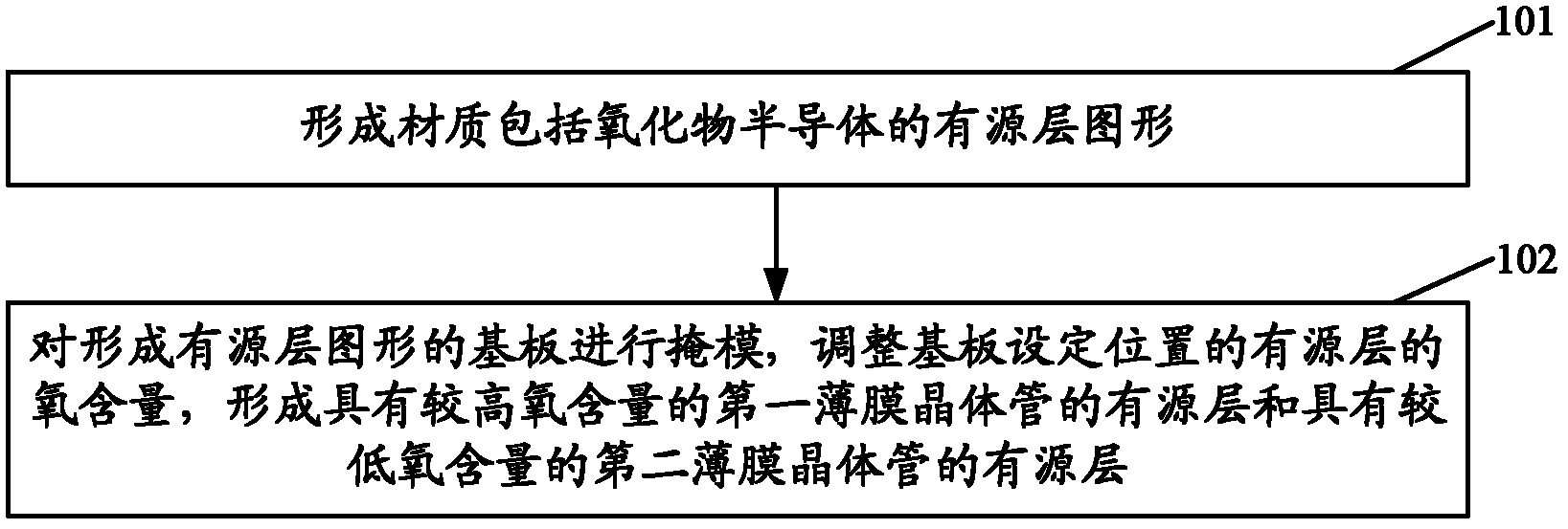
[0031] In order to solve the problem that IGZO semiconductor is used as the channel material of the active layer of the array substrate in the prior art, only its depletion or enhancement characteristics can only be used. The structure of the array substrate is relatively complicated, the stability is poor, and the effective pixel area cannot To further increase the technical problem, the present invention provides an array substrate and a manufacturing method thereof.

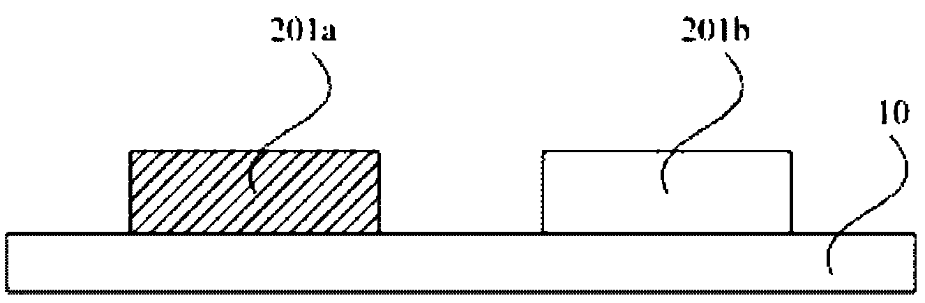
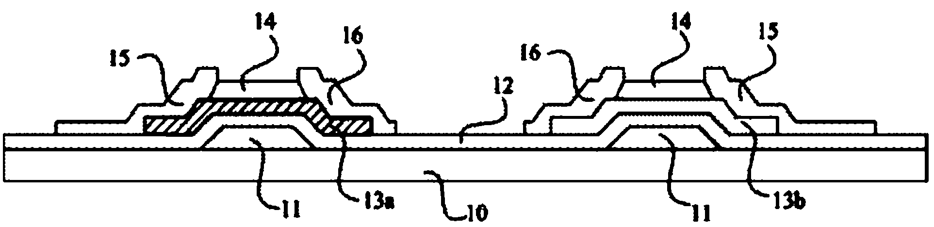
[0032] like figure 1 As shown, the array substrate of the present invention includes: a substrate 10 and a first thin film transistor 201a and a second thin film transistor 201b respectively located on the substrate 10, wherein the first thin film transistor 201a is an enhancement type, and the second thin film transistor 201b is depletion type.

[0033] The material of the active layer of the first thin film transistor 201a and the active layer of the second thin film transistor 201b includes an oxide semico...


PUM


Abstract

The invention discloses an array substrate and a manufacturing method of the array substrate. The array substrate comprises a substrate plate, a first TFT (thin film transistor) and a second TFT, wherein the first TFT and the second TFT are respectively arranged on the substrate plate, the first TFT is an enhancement type, and the second TFT is a depletion type. The array substrate plate is provided with the enhancement-type first TFT and the depletion-type second TFT at the same time at preset positions so as to exert the functional characteristics; and compared with a single depletion-type TFT or a single enhancement-type TFT of an array substrate in the prior art, the array substrate disclosed by the invention has the advantages of being capable of reducing the set number of TFTs and simplifying circuit wires so as to largely simplify a structure of the whole array substrate, largely improve the stability of the structure and further increase the effective pixel area of the array substrate.

Description

technical field [0001] The present invention relates to the field of display technology, in particular to an array substrate and a manufacturing method thereof. Background technique [0002] Thin Film Transistor (TFT for short) is one of the types of field effect transistors, and is mainly used in flat panel display devices. Thin Film Transistor Liquid Crystal Display (TFT-LCD for short) has the characteristics of small size, low power consumption, relatively low manufacturing cost and no radiation, and occupies a dominant position in the current flat panel display market. AMOLED (Active Matrix Organic Light Emitting Diode, active matrix organic light emitting diode, referred to as AMOLED) panel, known as the next generation display technology, compared with the traditional TFT-LCD panel, has the characteristics of fast response, high contrast, wide viewing angle, etc. . [0003] Oxide semiconductor indium gallium zinc oxide (InGaZnO4:IGZO) has been widely studied due to i...

Claims


Application Information

Patent Timeline
Patent Type & Authority Applications(China)
IPC IPC(8): H01L27/12H01L21/84
CPCH01L27/1225
Inventor 李延钊王刚黄国东田香军
Owner BOE TECH GRP CO LTD
Why Eureka
Try Eureka