TFT (thin film transistor) and manufacturing method thereof
A technology for thin film transistors and a manufacturing method, which is applied in the fields of transistors, semiconductor/solid-state device manufacturing, electrical components, etc., can solve the problems of inability to form ohmic contacts, poor contact performance, affecting the on-state current and stability of thin-film transistors, and the like. Uncontrollable composition, avoidance of influence, improved stability and effect of on-state current
- Summary
- Abstract
- Description
- Claims
- Application Information
AI Technical Summary
Problems solved by technology
Method used
Image


Examples
Embodiment approach 1
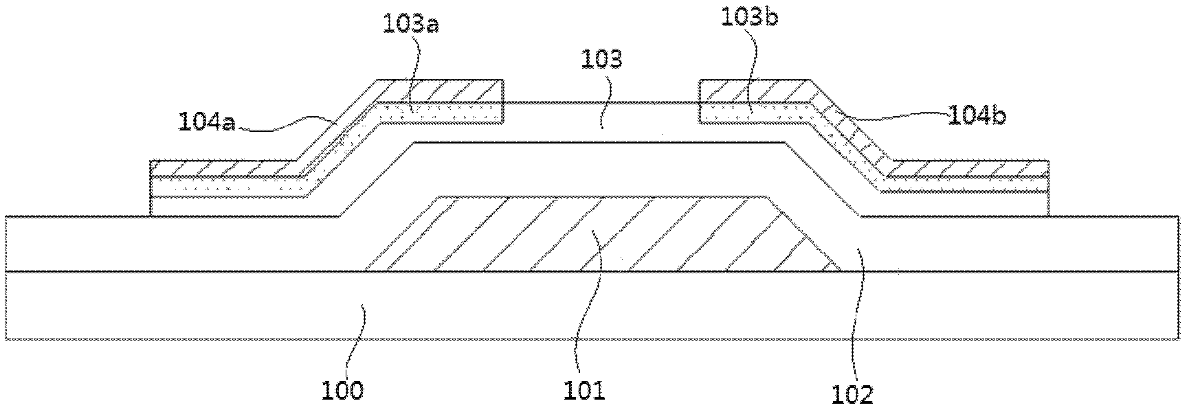
[0044] Such as figure 1 As shown, the thin film transistor of the present invention includes: a gate electrode layer 101 is disposed on a substrate 100, a gate insulating layer 102 is disposed on the gate electrode layer 101, and an oxide layer is disposed on the gate insulating layer 102. The semiconductor layer 103, that is, the active layer, is subjected to ion implantation or plasma treatment on both sides of the oxide semiconductor layer 103 to form a highly conductive first transition region 103a and a second transition region 103b, wherein the first transition region 103a and The second transition region 103b has the same elemental composition and resistivity. Between the first transition region 103a and the second transition region 103b is a channel region, a source electrode layer 104a is arranged on the first transition region 103a, and the first transition region 103a and the source electrode layer 104a An ohmic contact is formed between them, a drain electrode lay...
Embodiment approach 2
[0053] Such as Figure 2a-Figure 2d with figure 1 As shown, the manufacturing method of the thin film transistor of the present invention comprises:
[0054] Such as Figure 2a As shown, a gate electrode layer 101 is formed on a substrate 100;
[0055] Such as Figure 2b As shown, a gate insulating layer 102 is formed on the gate electrode layer 101;
[0056] Such as Figure 2c As shown, an oxide semiconductor layer 103 is formed on the gate insulating layer 102 by sputtering or other methods;
[0057] Such as Figure 2d As shown, a non-adjacent first transition region 103a and a second transition region 103b are formed on the oxide semiconductor layer 103 by means of ion implantation or plasma treatment, and the first transition region 103a and the second transition region 103a The resistivity of the transition region 103b is lower than the resistivity of the channel region between them;
[0058] Such as figure 1 As shown, a source electrode layer 104a is formed on t...
Embodiment approach 3
[0067] Such as image 3 As shown, the thin film transistor of the present invention includes: a buffer layer 201 is disposed on a substrate 200, an oxide semiconductor layer 202, that is, an active layer, is disposed on the buffer layer 201, and an oxide semiconductor layer 202 is disposed on the buffer layer 201. Ion implantation or plasma treatment is performed on both sides of the semiconductor layer 103 to form a highly conductive first transition region 202a and a second transition region 202b, wherein the first transition region 202a and the second transition region 202b have the same elemental composition and resistance Rate. Between the first transition region 202a and the second transition region 202b is a channel region, a source electrode layer 203a is arranged on the first transition region 202a, and the first transition region 202a and the source electrode layer 203a A contact region is formed between them, a drain electrode layer 203b is disposed on the second t...
PUM
 Abstract
Description
Claims
Application Information
 - R&D
- Intellectual Property
- Life Sciences
- Materials
- Tech Scout
- Unparalleled Data Quality
- Higher Quality Content
- 60% Fewer Hallucinations
Browse by: Latest US Patents, China's latest patents, Technical Efficacy Thesaurus, Application Domain, Technology Topic, Popular Technical Reports.
© 2025 PatSnap. All rights reserved.Legal|Privacy policy|Modern Slavery Act Transparency Statement|Sitemap|About US| Contact US: help@patsnap.com