Capacitive touch panels

A technology of electrodes and conductive inks, applied in the fields of electrical digital data processing, instruments, calculations, etc., can solve problems such as high cost, complicated operation, and small structure size

Active Publication Date: 2012-08-22
盈天实业(深圳)有限公司
View PDF5 Cites 12 Cited by
  • Summary
  • Abstract
  • Description
  • Claims
  • Application Information

AI Technical Summary

Problems solved by technology

[0009] According to existing known designs, the manufacturing process currently used to form the busbar structure in the metal layer and TCM layer is slow, complicated to operate, and environmentally destructive and expensive
Furthermore, due to the large number of steps involved in the process and the small size of the structures to be formed, errors are likely to occur in production resulting in defective products

Method used


Image

  • Capacitive touch panels
  • Capacitive touch panels
  • Capacitive touch panels

Examples


Embodiment Construction

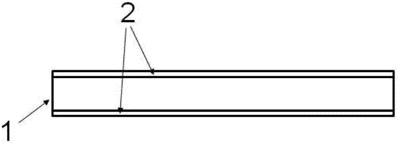
[0049] Depend on figure 1 As can be seen, the substrate 1 is transparent and may be rigid and made of glass or other inorganic transparent material such as silica, or may be flexible and made of such as (but not strictly limited to) polyester (PET) or polycarbonate Polyester (PC) polymer. The thickness of the substrate may range from one millimeter to several millimeters. A thin layer of transparent and electrically conductive material 2 is applied to both sides of the substrate. These TCM layers can be made, for example, from indium tin oxide (ITO), tin oxide (SnO 2 ), zinc oxide (ZnO) or other oxides, in which case they are called TCO (Transparent Conductive Oxide) and are used for example (without limitation) in Physical Vapor Deposition (PVD). Alternatively, other transparent conductive layers based on organic materials or nanoparticulate materials may also be used. The latter can be applied, for example, in movable type printing processes. Typical TCM layer thickness...


PUM

PropertyMeasurementUnit
thicknessaaaaaaaaaa
electrical resistanceaaaaaaaaaa

Abstract

A novel method and apparatus for performing the method is disclosed the apparatus comprises a laser (17), at least one ink jet print head (14), means for holding a transparent substrate having a transparent conductive layer, means (22) for adjusting the relative positions of the laser and at least one ink jet print head to the transparent conducting layer (2) and a controller to control the laser and ink jet print head whereby in a first step to inkjet print one or more coarse metal borders (15) onto the deposited TCM layer and in a second step by means of a single laser ablation process, ablating tracks in both the metal border and underlying TCM layer to form a plurality of discrete electrical busbars (12) and optionally also to form electrodes in the remainder of the TCM layer.

Description

technical field [0001] The present invention relates to improvements in capacitive touch screens, in particular the invention relates to surface electrodes and connecting edge busbars for use in capacitive touch screens and methods of providing such structures. Background technique [0002] Capacitive touch screen technology is used in a wide range of applications, such as mobile phones, satellite navigation systems, personal digital assistant (PDA) screens and handheld game consoles. [0003] One particular form of capacitive touchscreen is known as projected capacitive touchscreen technology or "PCT." In a PCT device, an XY array of sensing electrodes is formed in a layer of transparent conductive material. In use, a capacitance is formed between the user's finger and the projected capacitance from the sensing electrodes. Once a touch has occurred, it is precisely measured and translated into instructions, which are executed by the underlying electronics for the appropri...

Claims


Application Information

Patent Timeline
Patent Type & Authority Applications(China)
IPC IPC(8): G06F3/044
CPCG06F3/044Y10T29/49155Y10T29/5313G06F3/0446G06F3/0443G06F2203/04103
Inventor D·C·米尔恩
Owner 盈天实业(深圳)有限公司
Why Eureka
Try Eureka