Poly-silicon resistor structure and produciton method thereof

A technology of polysilicon resistors and manufacturing methods, which is applied in semiconductor/solid-state device manufacturing, electric solid-state devices, circuits, etc., and can solve the problems of occupying device space, insufficient resistance, and large size

Active Publication Date: 2012-09-12
SHANGHAI HUAHONG GRACE SEMICON MFG CORP
View PDF4 Cites 14 Cited by
  • Summary
  • Abstract
  • Description
  • Claims
  • Application Information

AI Technical Summary

Problems solved by technology

[0007] Moreover, the resistance value of the polysilicon resistor of the prior art is easily affected by temperature, and the square resistance of the polysilicon resistor of

Method used


Image

  • Poly-silicon resistor structure and produciton method thereof
  • Poly-silicon resistor structure and produciton method thereof
  • Poly-silicon resistor structure and produciton method thereof

Examples


Embodiment Construction

[0030] In order to make the content of the present invention clearer and easier to understand, the content of the present invention will be described in detail below in conjunction with specific embodiments and accompanying drawings.

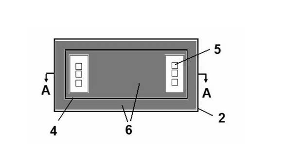
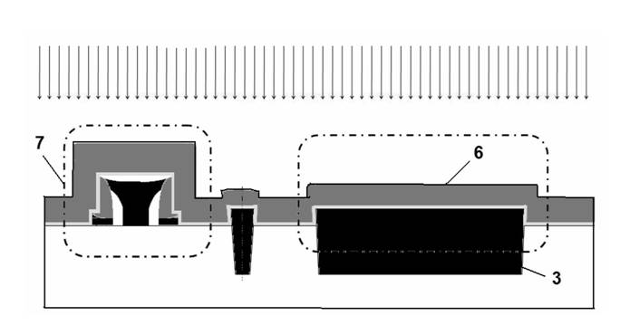
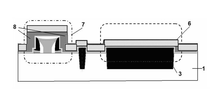
[0031] Figure 3 to Figure 8 A method for manufacturing a polysilicon resistor structure taken along a second direction (a direction perpendicular to the direction A-A is taken) according to an embodiment of the present invention is schematically shown. where, as an example, Figure 4 to Figure 8 The polysilicon resistor structure and the memory cell structure according to the embodiment of the present invention ( Figure 4 The structure framed by the dotted box on the left shown) is shown in combination. However, those skilled in the art can understand that the polysilicon resistor structure according to the embodiments of the present invention can also be used in any other suitable semiconductor devices or circuits.

[0032] The invention p...


PUM


Abstract

The invention provides a poly-silicon resistor structure and a production method thereof. According to the invention, the production method of the poly-silicon resistor structure capable of adjusting resistance and temperature coefficient of a poly-silicon resistor comprises the following steps of: forming an insulation area in a substrate, wherein the insulation area is exposed or extends out of the surface of the substrate; forming a first poly-silicon layer on the surface of a silicon wafer, wherein the first poly-silicon layer covers the insulation area, and is an in-situ doped n-type poly-silicon layer; injecting P-type doped ions into the first poly-silicon layer, so as to neutralize N-type doped ions in the former first poly-silicon layer; etching the first poly-silicon layer subjected to an injection, so that the first poly-silicon layer on the insulation area is reversed; isolating the first poly-silicon layer from a second poly-silicon layer formed next; forming the second poly-silicon layer on the surface of the silicon wafer; and etching the second poly-silicon layer.

Description

technical field [0001] The invention relates to the field of semiconductor manufacturing, and more specifically, the invention relates to a polysilicon resistor structure and a manufacturing method of the polysilicon resistor structure. Background technique [0002] In semiconductor chip circuit design, a large number of polysilicon resistors are used. Generally, circuit designers use traditional n-type or p-type polycrystalline resistors, but these resistors require a silicide barrier layer in the manufacturing process, that is, an additional photolithography step is required. The storage polysilicon resistance proposed in the improvement scheme of the prior art does not require a silicide barrier layer, which reduces the manufacturing cost. However, the polysilicon resistor is an n-type resistor with a large temperature coefficient; in addition, the polysilicon has a high doping concentration, so the resistance value is small, which is not conducive to reducing the circui...

Claims


Application Information

Patent Timeline
IPC IPC(8): H01L27/06H01L27/08H01L21/02
Inventor 李冰寒江红
Owner SHANGHAI HUAHONG GRACE SEMICON MFG CORP
Why Eureka
Try Eureka