Device for improving properties of light spot of super-resolution phase board

A phase plate and super-resolution technology, applied in optics, optical components, nonlinear optics, etc., can solve problems such as reducing signal-to-noise ratio

Inactive Publication Date: 2012-09-19
SHANGHAI INST OF OPTICS & FINE MECHANICS CHINESE ACAD OF SCI
View PDF4 Cites 5 Cited by
  • Summary
  • Abstract
  • Description
  • Claims
  • Application Information

AI Technical Summary

Problems solved by technology

But the disadvantage is that it increases the side lobe while compre

Method used


Image

  • Device for improving properties of light spot of super-resolution phase board
  • Device for improving properties of light spot of super-resolution phase board
  • Device for improving properties of light spot of super-resolution phase board

Examples


Embodiment Construction

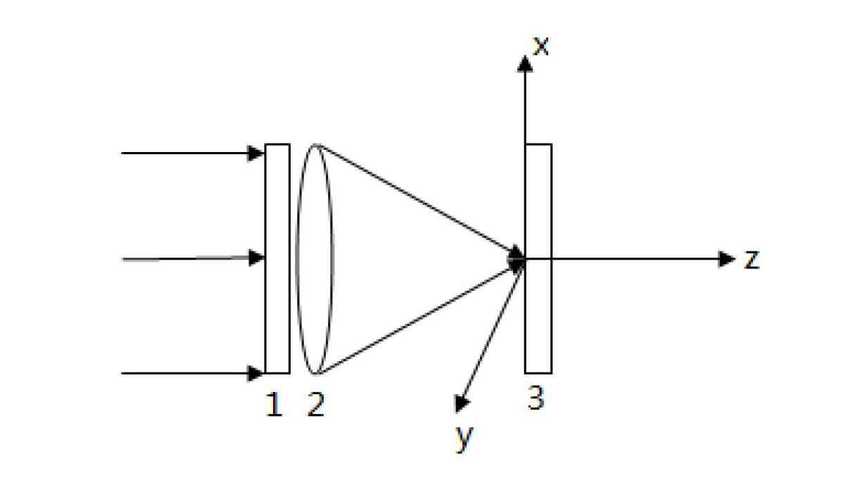
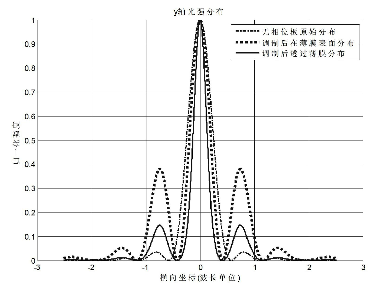
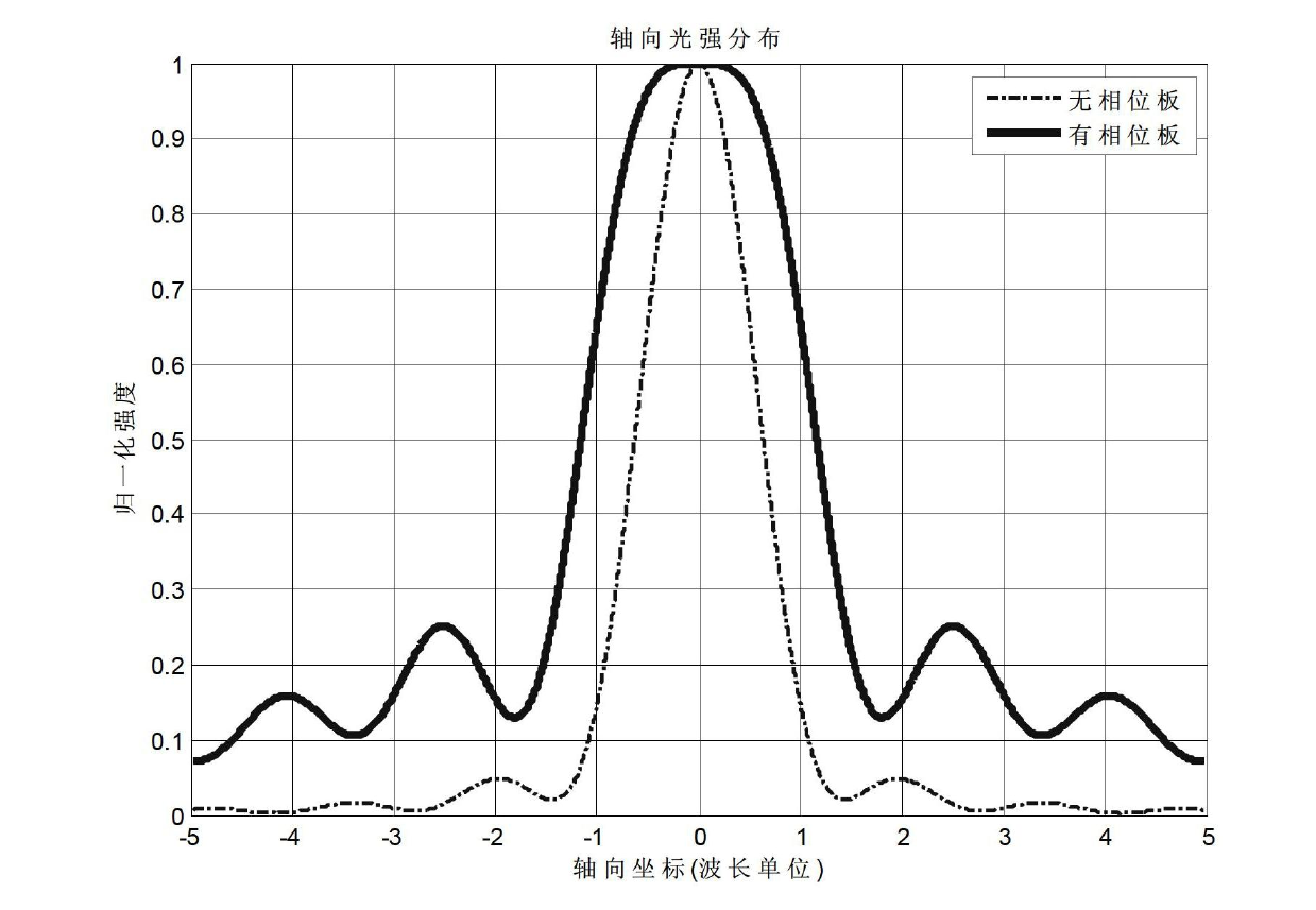
[0015] figure 1 It is a structural principle diagram of a specific embodiment of the present invention. Depend on figure 1 It can be seen that the composition of the device for improving the spot performance of the super-resolution phase plate in the present invention: along the beam advancing direction, there are three-ring pure phase type super-resolution phase plate 1, objective lens 2 with numerical aperture NA=0.95, Sb 2 Te 3 Non-linear saturable absorption film 3, the normalized radius of the three-ring phase-only super-resolution phase plate 1 is r1=0.13, r2=0.47, r3=1; the phases of the three regions are: φ 1 =0, φ 2 = π, φ 3 =0; the objective lens 2 is in close contact with the three-ring pure phase super-resolution phase plate 1, and the Sb 2 Te 3 The nonlinear saturable absorption film 3 is located at the focal plane of the objective lens 2, the Sb 2 Te 3 The selection range of the thickness of the nonlinear saturable absorption film is 10~100nm, and the lin...


PUM


Abstract

The invention provides a device for improving properties of light spots of a super-resolution phase board. The device is characterized by consisting of a three-ring pure-phase type super-resolution phase board, an object lens with a numerical aperture NA of 0.95, and a Sb2Te3 non-linear saturated absorption thin film in sequence along a light beam forward direction; normalized radii of the three-ring pure-phase type super-resolution phase board are r1 of 0.13, r2 of 0.47 and r3 of 1 respectively; phases of three areas respectively are phi1 of 0, phi2 of pi, and phi3 of 0; the object lens is tightly adhered to the three-ring pure-phase type super-resolution phase board; the Sb2Te3 non-linear saturated absorption thin film is located on a focal plane of the object lens; the thickness of the Sb2Te3 non-linear saturated absorption thin film has a selection range of 10-100 nm; and a linear absorption coefficient and a non-linear absorption coefficient of the Sb2Te3 non-linear saturated absorption thin film respectively are alpha0 of 5*10<7>/m and beta of -2*10<-2>m/w respectively. According to the device provided by the invention, the light spots and sidelobes are further reduced and a focal depth is lengthened.

Description

technical field [0001] The invention relates to the fields of photolithography, optical imaging and information storage. Background technique [0002] With the rapid development of micro-nano technology, optical storage technology, lithography technology, optical imaging technology, and optical manufacturing technology are all facing the problem of breaking through the diffraction limit. By shortening the laser wavelength to 405nm of the GaN laser and increasing the numerical aperture of the optical head to 0.95, the diffraction spot size formula: D=0.61λ / N.A. The diffraction spot can only reach about 0.5μm, when using visible light wavelength and far-field optics Under the system, relying on the traditional method of shortening the laser wavelength and increasing the numerical aperture of the optical head has gone to the limit. How to break the diffraction limit of light and make the light spot reach the nanometer level is the current bottleneck problem. [0003] It is a ...

Claims


Application Information

Patent Timeline
IPC IPC(8): G02B27/48G02B27/58G02F1/35
Inventor 查一昆魏劲松干福熹
Owner SHANGHAI INST OF OPTICS & FINE MECHANICS CHINESE ACAD OF SCI
Why Eureka
Try Eureka