Strain SiGe plane Si-based BiCMOS (Bipolar Complementary Metal Oxide Semiconductor) integrated device on basis of SOI (Silicon On Insulator) substrate and preparation method

A technology for integrating devices and substrate surfaces, which is applied in the field of strained SiGe planar Si-based BiCMOS integrated devices and preparation, and can solve problems such as difficult to meet design, affect device performance, and unsatisfactory photolithography technology

Inactive Publication Date: 2012-10-17
XIDIAN UNIV
View PDF3 Cites 0 Cited by
  • Summary
  • Abstract
  • Description
  • Claims
  • Application Information

AI Technical Summary

Problems solved by technology

For example, when the feature size is less than 100nm, due to problems such as tunneling leakage current and reliability, the traditional gate dielectric material SiO 2 Unable to meet the requirements of low power consumption; the short channel effect and narrow channel effect of nanometer devices are becoming more and more obvious, which seriously affects the device performance; traditional lithography technology cannot meet the shrinking lithography precision
Therefore, traditional Si-based process devices are increasingly difficult to meet the needs of design

Method used


Image

  • Strain SiGe plane Si-based BiCMOS (Bipolar Complementary Metal Oxide Semiconductor) integrated device on basis of SOI (Silicon On Insulator) substrate and preparation method

Examples


Embodiment 1

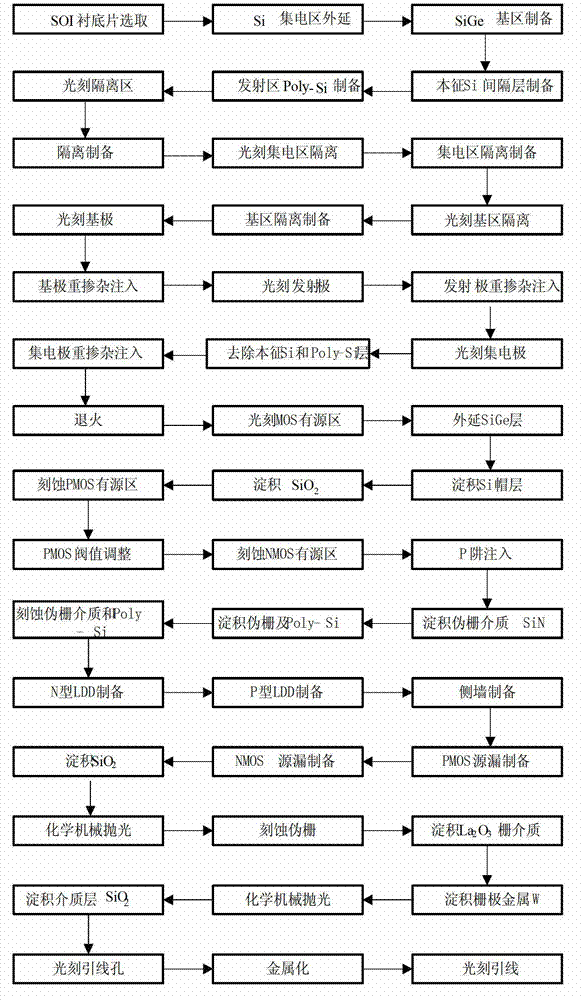
[0113] Embodiment 1: The strained SiGe planar Si-based BiCMOS integrated device and circuit based on the SOI substrate with a channel length of 22nm are prepared, and the specific steps are as follows:

[0114] Step 1, epitaxial growth.

[0115] (1a) Select the SOI substrate, the support material of the lower layer of the substrate is Si, and the middle layer is SiO 2 , with a thickness of 150nm, and the upper material is doped with a concentration of 1×10 16 cm -3 N-type Si with a thickness of 100nm;

[0116] (1b) Using the method of chemical vapor deposition (CVD), grow a layer of N-type epitaxial Si layer with a thickness of 250nm on the upper layer of Si material at 600°C, as the collector region, and the doping concentration of this layer is 1× 10 16 cm -3 ;

[0117] (1c) Deposit a layer of SiO with a thickness of 200nm on the surface of the substrate at 600°C by chemical vapor deposition (CVD). 2 layer;

[0118] (1d) Deposit a layer of SiN with a thickness of 100...

Embodiment 2

[0176] Embodiment 2: The strained SiGe planar Si-based BiCMOS integrated device and circuit based on the SOI substrate with a channel length of 130nm are prepared, and the specific steps are as follows:

[0177] Step 1, epitaxial growth.

[0178] (1a) Select the SOI substrate, the support material of the lower layer of the substrate is Si, and the middle layer is SiO 2 , with a thickness of 300nm, and the upper material is doped with a concentration of 5×10 16 cm -3 N-type Si with a thickness of 120nm;

[0179] (1b) Using the chemical vapor deposition (CVD) method, at 700 ° C, grow a layer of N-type epitaxial Si layer with a thickness of 250 nm on the upper Si material, as the collector region, and the doping concentration of this layer is 5× 10 16 cm -3 ;

[0180] (1c) Deposit a layer of SiO with a thickness of 240nm on the surface of the substrate at 700°C by chemical vapor deposition (CVD). 2 layer;

[0181] (1d) Deposit a layer of SiN with a thickness of 150 nm on ...

Embodiment 3

[0239] Embodiment 3: The strained SiGe planar Si-based BiCMOS integrated device and circuit based on the SOI substrate with a channel length of 350nm are prepared, and the specific steps are as follows:

[0240] Step 1, epitaxial growth.

[0241] (1a) Select the SOI substrate, the support material of the lower layer of the substrate is Si, and the middle layer is SiO 2 , with a thickness of 400nm, and the upper material is doped with a concentration of 1×10 17 cm -3 N-type Si with a thickness of 150nm;

[0242] (1b) Using chemical vapor deposition (CVD), grow a layer of N-type epitaxial Si layer with a thickness of 300nm on the upper layer of Si material at 750°C, as the collector region, and the doping concentration of this layer is 1× 10 17 cm -3 ;

[0243] (1c) Deposit a layer of SiO with a thickness of 300nm on the surface of the substrate at 800°C by chemical vapor deposition (CVD). 2 layer;

[0244] (1d) Deposit a SiN layer with a thickness of 200nm on the surfac...


PUM

PropertyMeasurementUnit
thicknessaaaaaaaaaa
thicknessaaaaaaaaaa
thicknessaaaaaaaaaa

Abstract

The invention discloses a strain SiGe plane Si-based BiCMOS (Bipolar Complementary Metal Oxide Semiconductor) integrated device on the basis of a SOI (Silicon On Insulator) substrate and a preparation method. The preparation method has the following preparation process of: growing an N-Si layer on the SOI substrate to form a bipolar device collector region, photoetching a base region, regionally growing a P-SiGe layer, an i-Si layer and an i-Poly-Si layer in the base region, preparing a deep-trench isolation, forming an emitting electrode, a base electrode and a collector electrode and forming a SiGe HBT (Heterojunction Bipolar Trthissistor) device; and growing a strain SiGe material on the substrate, forming active regions of NMOS (N-channel Metal Oxide Semiconductor) and PMOS (P-channel Metal Oxide Semiconductor) devices, preparing a pseudo-gate, carrying out self-aligning to generate source drain regions of the NMOS and PMOS devices, removing the pseudo-gate, preparing a grid electrode and photoetching leads to form the strain SiGe plane Si-based BiCMOS integrated device on the basis of the SOI substrate and a circuit. According to the method, the SOI SiGe BiCMOS integrated circuit is prepared by sufficiently utilizing the characteristic that the hole mobility of a SiGe material is higher than that of a common Si material, so that the performance of the existing analog and analog-digital mixed integrated circuit is greatly improved.

Description

technical field [0001] The invention belongs to the technical field of semiconductor integrated circuits, and in particular relates to a strained SiGe planar Si-based BiCMOS integrated device based on an SOI substrate and a preparation method. Background technique [0002] Semiconductor integrated circuit technology is the core technology of high-tech and information industries, and has become an important symbol to measure a country's scientific and technological level, comprehensive national strength and national defense strength, while microelectronic technology represented by integrated circuits is the key to semiconductor technology. The semiconductor industry is the basic industry of the country. The reason why it develops so fast is not only the huge contribution of technology itself to economic development, but also its wide applicability. [0003] Gordon Moore, one of the founders of Intel, proposed "Moore's Law" in 1965, which states that the number of transistors ...

Claims


Application Information

Patent Timeline
Patent Type & Authority Applications(China)
IPC IPC(8): H01L27/12H01L21/84H01L21/28
Inventor 张鹤鸣周春宇宋建军舒斌胡辉勇宣荣喜戴显英郝跃
Owner XIDIAN UNIV
Why Eureka
Try Eureka