Semiconductor device and manufacturing method thereof

A manufacturing method and semiconductor technology, which is applied in the direction of semiconductor/solid-state device manufacturing, semiconductor devices, electrical components, etc., can solve problems such as not being able to meet the stress requirements of devices, and achieve the effects of enhancing stress, increasing stress, and enhancing stress

Active Publication Date: 2012-10-17
INST OF MICROELECTRONICS CHINESE ACAD OF SCI
View PDF5 Cites 2 Cited by
  • Summary
  • Abstract
  • Description
  • Claims
  • Application Information

AI Technical Summary

Problems solved by technology

[0006] The embodiment of the present invention provides a semiconductor device and its manufacturing method, which solves the problem that the existing silicon nitride film layer cannot meet the stress requirements of the device

Method used


Image

  • Semiconductor device and manufacturing method thereof
  • Semiconductor device and manufacturing method thereof
  • Semiconductor device and manufacturing method thereof

Examples


no. 1 example

[0075] The following combination Figure 3-Figure 9 The first embodiment of the semiconductor device manufacturing method of the above-mentioned embodiments will be described in detail.

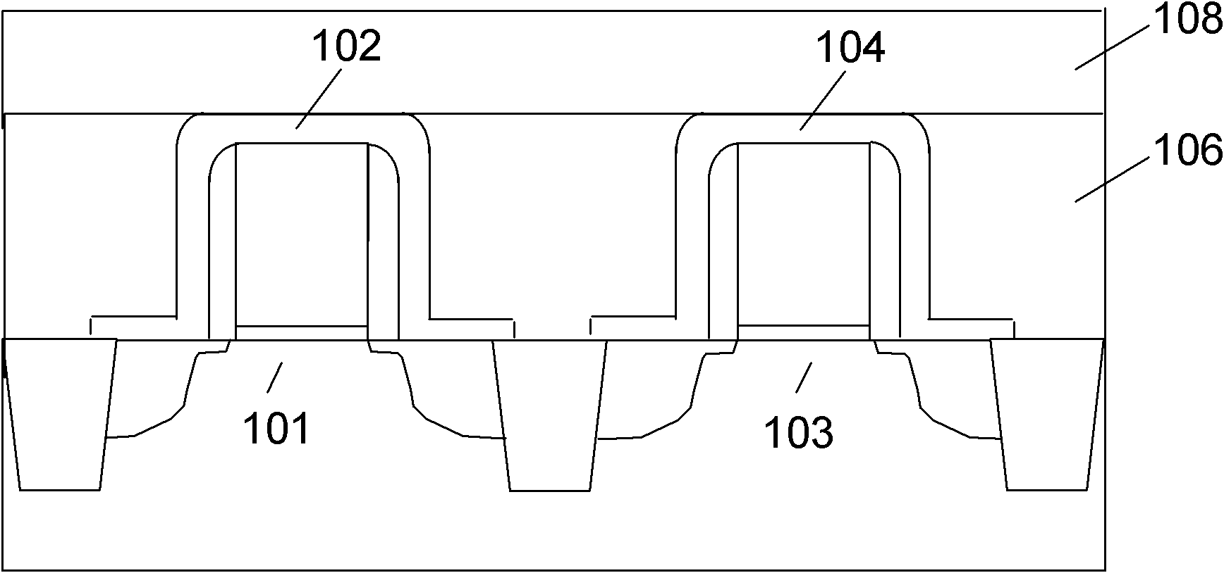
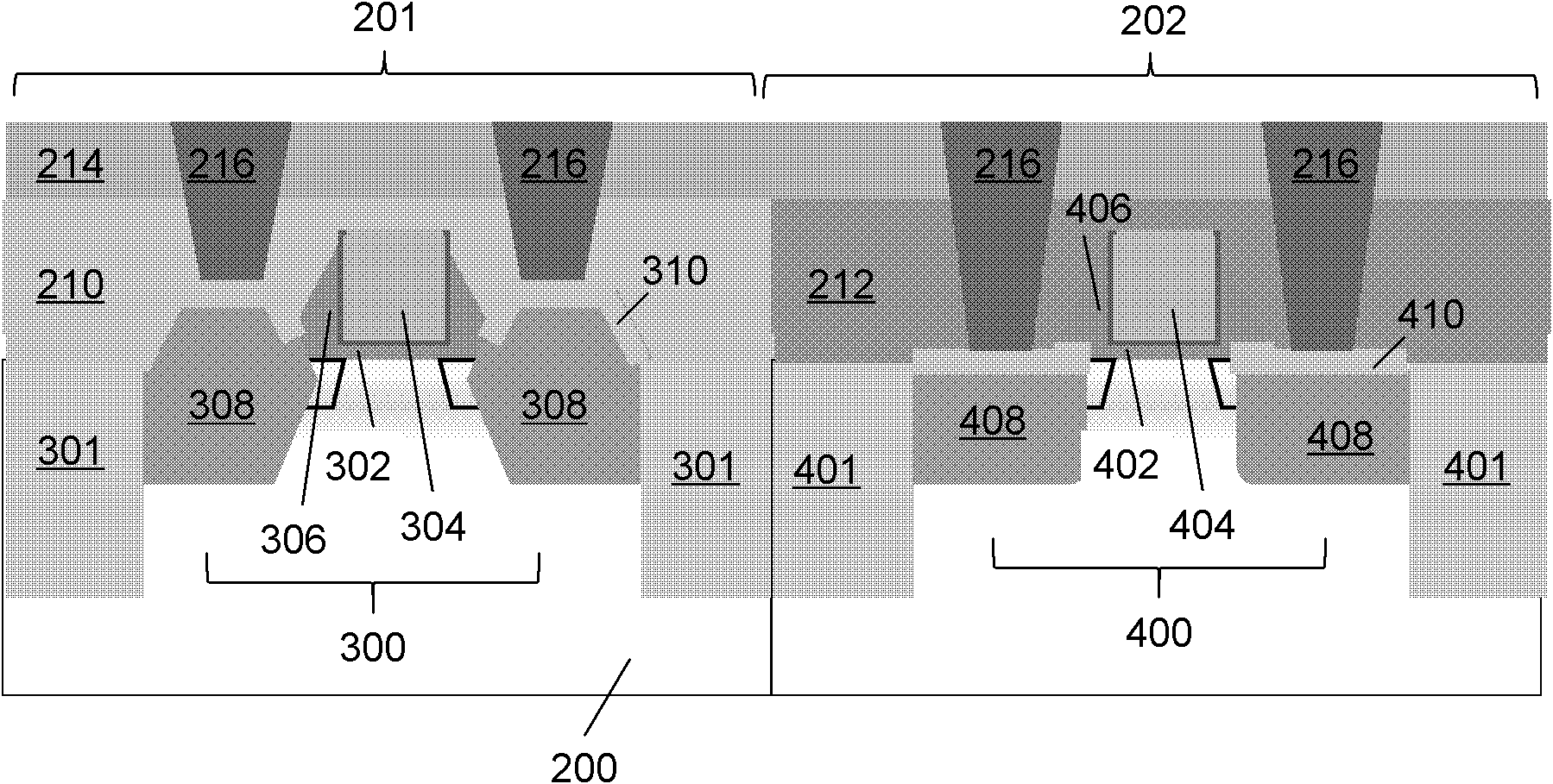
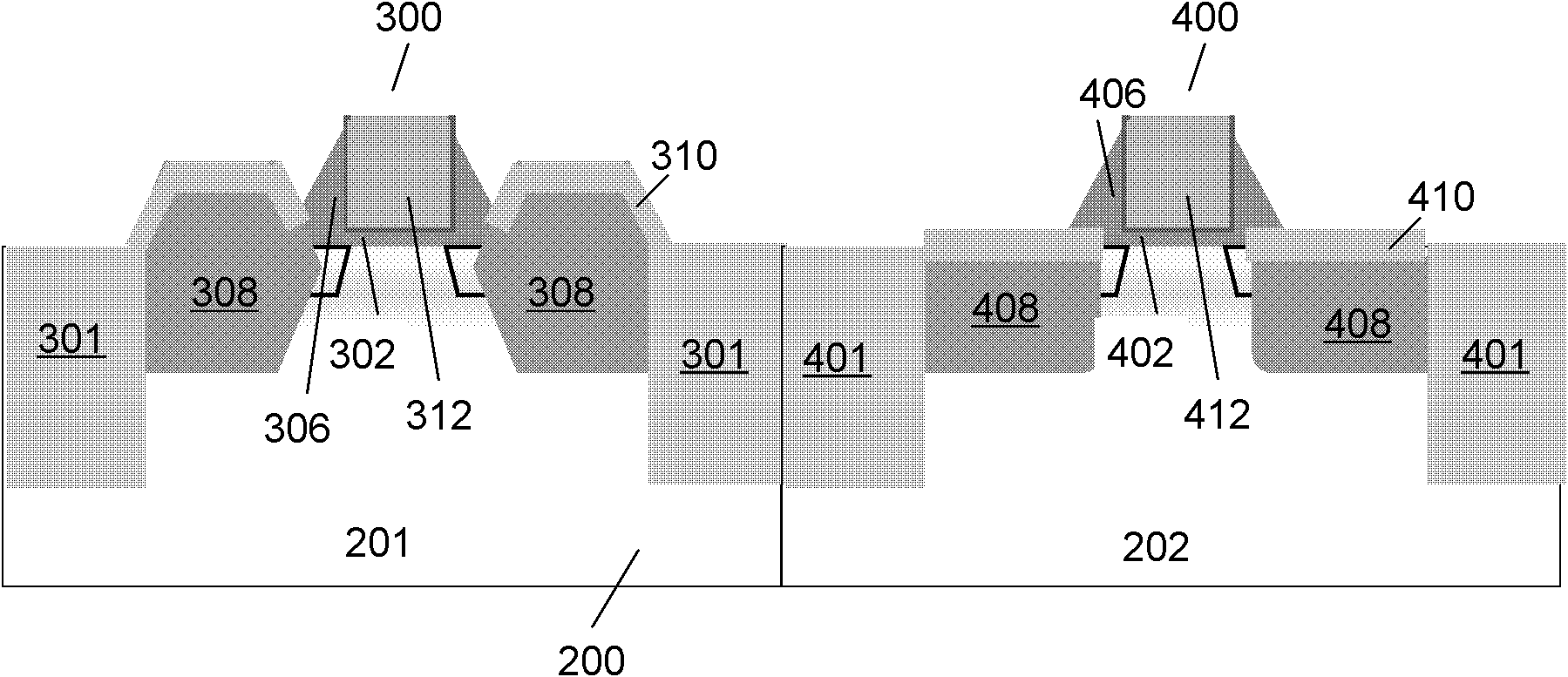
[0076] First, refer to image 3 , in step S11 , providing a substrate 200 including an NMOS region 202 and a PMOS region 201 .

[0077] In this embodiment, the substrate 200 is a silicon substrate, and an N well and a P well can be formed respectively by performing well doping on the substrate, wherein the N well will be used to form a PMOS device, and the P well will be used to form a PMOS device. It will be used to form NMOS devices, therefore, in this embodiment, the N well can be understood as the PMOS region 201 , and the P well can be understood as the NMOS region 202 . At the same time, isolation regions 301 and 401 are formed on the substrate 200, and the isolation regions may include silicon dioxide or other materials that can separate active regions of devices.

[0078] Then, ref...

no. 2 example

[0095] The first embodiment in which the semiconductor device of the present invention is formed by using the gate-last process has been described in detail above, and only the differences between the second embodiment and the first embodiment will be described below. Parts not described should be considered to be performed using the same steps, methods or processes as those in the first embodiment, so details will not be repeated here.

[0096] First, refer to Figure 10 , in step S21 , providing a substrate 200 including an NMOS region 202 and a PMOS region 201 . It is the same as step S11 in the first embodiment, and will not be repeated here.

[0097] Then, refer to Figure 10 , in step S22 , the NMOS device 400 in the NMOS region 202 and the PMOS device 300 in the PMOS region 201 are provided. Only the step of forming the gate stack is different from the step S12 of the first embodiment, and other steps are the same, and will not be repeated here. In this embodiment, ...


PUM

PropertyMeasurementUnit
Thicknessaaaaaaaaaa

Abstract

A semiconductor device and a manufacturing method thereof are disclosed. The semiconductor device comprises a substrate, a field effect transistor in the substrate, a first interlayer dielectric layer on the field effect transistor and a second interlayer dielectric layer on the first interlayer dielectric layer, wherein the first interlayer dielectric layer is a stress dielectric material. The first interlayer dielectric layer on the field effect transistor is used to increase a stress effect on the field effect transistor, wherein the first interlayer dielectric layer is the stress dielectric material. Through increasing a volume of interaction space, the stress to the device is enhanced. A problem that a stress demand of the device can not be satisfied because the space is reduced is solved.

Description

technical field [0001] The present invention relates to semiconductor structure and manufacturing technology, more specifically, to a semiconductor device and its manufacturing method. Background technique [0002] With the rapid development of semiconductor technology, the feature size of semiconductor devices is shrinking continuously, which makes the integration level of integrated circuits higher and higher, which also puts forward higher requirements for the performance of devices. [0003] Among other things, mechanical stress within a semiconductor device substrate can be used to tune device performance. For a Complementary Metal Oxide Semiconductor Field Effect Transistor (CMOS), the mobility of carriers can be improved by enhancing the stress of the channel. For example, in a silicon wafer, when the channel of the NMOS device has a tensile stress, the electron mobility of the NMOS device can be improved, and when the channel of the PMOS device has a compressive str...

Claims


Application Information

Patent Timeline
IPC IPC(8): H01L29/78H01L21/336
Inventor 殷华湘徐秋霞陈大鹏
Owner INST OF MICROELECTRONICS CHINESE ACAD OF SCI
Why Eureka
Try Eureka