Formation method for semiconductor structure

A semiconductor and patterning technology, which is applied in semiconductor devices, semiconductor/solid-state device manufacturing, electrical components, etc., can solve the problem of poor stress effect of the stress layer 11, influence of the shape of the source and drain grooves, and influence on the performance of fin field effect transistors and other issues to achieve the effect of improving stress and performance

Active Publication Date: 2017-07-14
SEMICON MFG INT (SHANGHAI) CORP +1
View PDF4 Cites 4 Cited by
  • Summary
  • Abstract
  • Description
  • Claims
  • Application Information

AI Technical Summary

Problems solved by technology

In the process of forming the polysilicon gates 21 across the fins 10, in order to improve the pattern uniformity of the polysilicon gates 21, shallow trench isolation between adjacent fins 10 arranged along the length direction of the fins 10 is usually performed. A dummy polysilicon gate 22 is formed on the surface of the structure 20. Since the surface of the shallow trench isolation structure 20 is lower than the top surface of the fin 10, the bottom of the dummy polysilicon gate 22 is also lower than the top surface of the fin 10, causing the dummy gate 22 There is a gap between the fin and t

Method used


Image

  • Formation method for semiconductor structure
  • Formation method for semiconductor structure
  • Formation method for semiconductor structure

Examples


Embodiment Construction

[0031] As mentioned in the background art, the performance of the semiconductor structure formed in the prior art needs to be further improved.

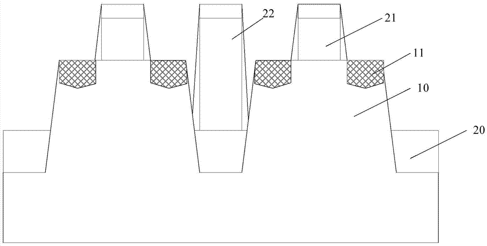
[0032] In the embodiment of the present invention, dummy gates are formed on the surface of the shallow trench isolation structure that has not been etched back, so as to avoid affecting the morphology of the source and drain grooves in the subsequent process of forming the source and drain grooves.

[0033] In order to make the above objects, features and advantages of the present invention more comprehensible, specific embodiments of the present invention will be described in detail below in conjunction with the accompanying drawings.

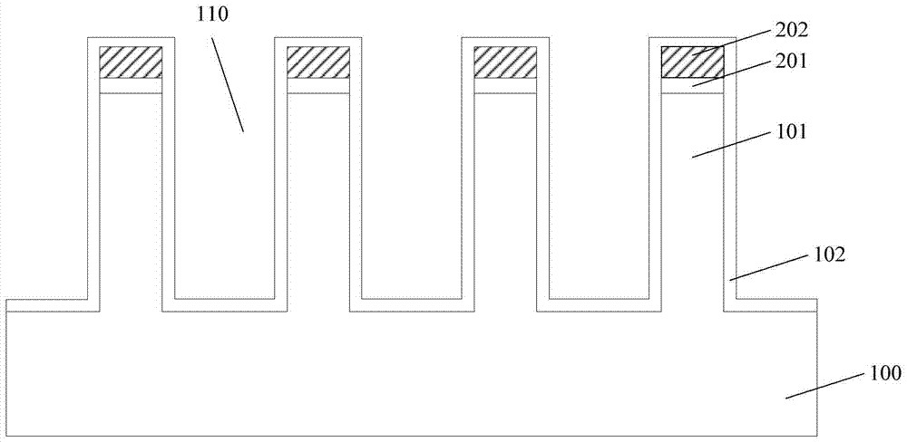
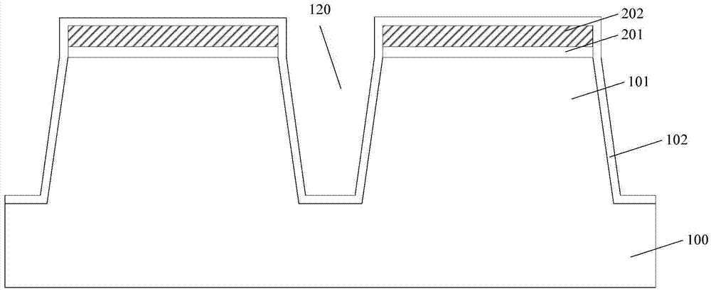
[0034] Please refer to figure 2 and image 3 A semiconductor substrate 100 is provided, and the semiconductor substrate 100 is etched to form several fins 101. The top of the fins 101 has a mask layer 202, and between adjacent fins 101 there are first fins 101 arranged along the length direction o...


PUM


Abstract

Disclosed is a formation method for a semiconductor structure. The formation method comprises the steps of providing a semiconductor substrate; forming a plurality of fin parts, wherein a mask layer is arranged on the top arts of the fin parts, and first grooves and second grooves are formed between adjacent fin parts; forming an isolating layer in the first grooves and the second grooves; removing the mask layer to form a first dielectric layer and a second dielectric layer which cover the isolating layer and the fin parts; forming a patterned mask layer with openings on the surface of the second dielectric layer; performing ion implantation on the second dielectric layer along the openings; removing the patterned mask layer and performing annealing treatment to form a doping layer in the second dielectric layer, wherein the etching rate of the doping layer is less than that of the second dielectric layer; removing the second dielectric layer and a part of the doping layer of certain thickness; etching the first dielectric layer and remaining a part of the first dielectric layer of certain thickness; and etching the isolating layer to reduce the height, outside the second grooves, of the isolating layer. By virtue of the formation method, the non-etched isolating layer is formed, and a pseudo gate is formed on the surface of the non-etched isolating layer, so that performance of a to-be-formed transistor can be improved.

Description

technical field [0001] The invention relates to the technical field of semiconductors, in particular to a method for forming a semiconductor structure. Background technique [0002] With the continuous development of semiconductor process technology, the process node is gradually reduced, and the gate-last (gate-last) process has been widely used to obtain an ideal threshold voltage and improve device performance. However, when the feature size (CD, Critical Dimension) of the device is further reduced, even if the gate-last process is adopted, the structure of the conventional MOS field effect transistor can no longer meet the requirements for device performance, and the fin field effect transistor (Fin FET) as Substitution of conventional devices has received extensive attention. [0003] In order to further improve the performance of fin field effect transistors, stress engineering is introduced into the transistor manufacturing process. After the source and drain grooves...

Claims


Application Information

Patent Timeline
IPC IPC(8): H01L21/336H01L29/78
CPCH01L29/66545H01L29/66803H01L29/7848H01L29/785
Inventor 赵海
Owner SEMICON MFG INT (SHANGHAI) CORP
Why Eureka
Try Eureka