A kind of Sonos flash memory and its preparation method and operation method

A memory and flash technology, which is applied in the field of non-volatile semiconductor memory, can solve the problems of high power consumption, difficulty in continuing to scale, and low programming efficiency, and achieve the effects of reducing power consumption, reducing drain current, and improving programming efficiency

Active Publication Date: 2015-07-29
PEKING UNIV
View PDF5 Cites 0 Cited by
  • Summary
  • Abstract
  • Description
  • Claims
  • Application Information

AI Technical Summary

Problems solved by technology

However, due to the limitation of the most basic programming mechanism, this SONOS-structured flash memory also has the same problems as the first type of flash memory, such as low programming efficiency, high power consumption, and difficulty in scaling down.

Method used


Image

  • A kind of Sonos flash memory and its preparation method and operation method
  • A kind of Sonos flash memory and its preparation method and operation method
  • A kind of Sonos flash memory and its preparation method and operation method

Examples


Embodiment Construction

[0042] Below in conjunction with the accompanying drawings, the flash memory of the P-type silicon substrate is taken as an example to further illustrate the preparation of the flash memory of the present invention and the basic working mode of the flash memory, but the scope of the present invention is not limited thereby. , the present invention is also applicable to the flash memory with N-type silicon as the substrate.

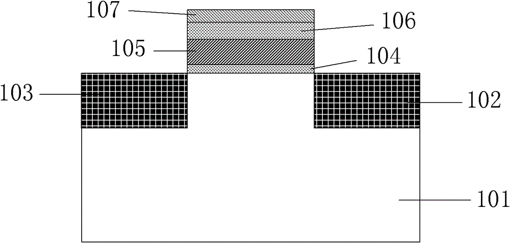
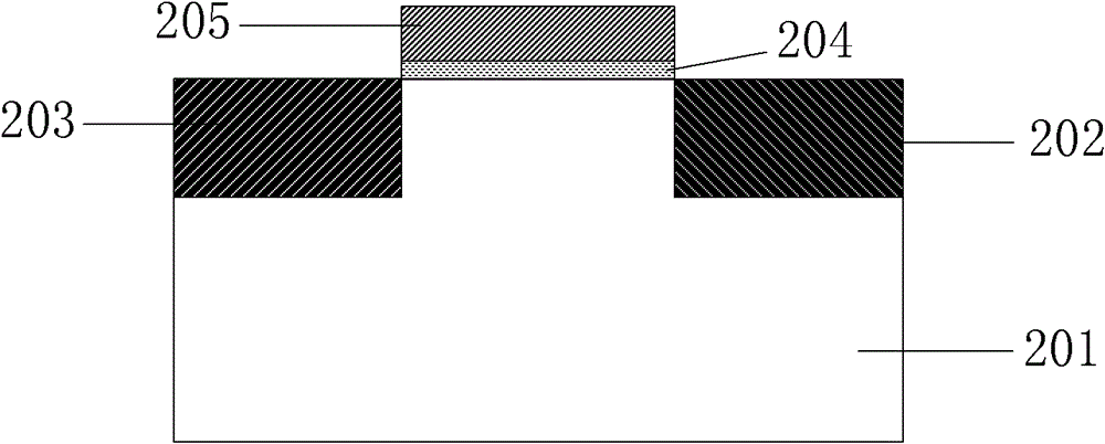
[0043] The structure of the flash memory prepared in this embodiment is as follows Figure 4 As shown, the P-type silicon 401 is used as the substrate, the two ends of the silicon plane are the P+ region and the N+ region, the middle is the channel region, and the tunneling oxide layer, the silicon nitride trap layer, and the blocking oxidation layer and the polysilicon control gate. The whole device is a TFET type SONOS flash memory.

[0044] The preparation of above-mentioned flash memory comprises the following steps:

[0045] (1) performing shallow ...


PUM


Abstract

A SONOS flash memory device, a manufacturing method and an operation method therefor, comprising a substrate (401), a source and drain (402 and 403), and a channel. Sequentially provided on the channel are a tunneled oxide layer (404), a silicon nitride trap layer (405), a blocking oxide layer (406), and a polycrystalline control gate (407). The SONOS flash memory device is characterized in that: the substrate (401) is of lightly doped silicon, and the source and drain (402 and 403) are of different doping types, being respectively a P+ region and an N+ region. The device is provided with improved compatibility with existing standard CMOS techniques, thus allowing for effectively increased programming efficiency, reduced power consumption, inhibited feedthrough effect, and a compact size.

Description

technical field [0001] The invention belongs to the technical field of non-volatile semiconductor memory in VLSI, in particular to a SONOS type flash memory using TFET (Tunneling Field Effective Transistor). Background technique [0002] At a time when various consumer electronics products are on the rise, the market demand for non-volatile semiconductor memory is also increasing. As a very important non-volatile memory, flash memory has recently become the darling of the industry. [0003] Flash memory (Flash Memory, also known as flash memory) has been around for decades since its appearance. During this period, while it has been widely used, it has also been continuously improved. In chronological order, the following two basic forms appear in turn: [0004] 1. Floating Gate Flash Memory [0005] This structure of flash memory uses polysilicon floating gates to store electrons. Its specific structure is as figure 1 As shown, on the bulk silicon substrate 101 , in ad...

Claims


Application Information

Patent Timeline
Patent Type & Authority Patents(China)
IPC IPC(8): H01L29/792H01L21/336G11C16/04
CPCH01L21/28282H01L29/792G11C16/0466H01L29/40117
Inventor 秦石强田明唐粕人唐昱蔡一茂黄如
Owner PEKING UNIV
Why Eureka
Try Eureka