Vanadium dioxide-based composite film with adjustable radiance as well as preparation method and application thereof
A technology of vanadium dioxide and composite film, applied in the field of vanadium dioxide-based composite film and its preparation, can solve the problems of weakening visible light transmittance, increasing reflection and absorption, etc., achieving excellent thermochromic performance, improving thermal insulation performance, low radiation effect
- Summary
- Abstract
- Description
- Claims
- Application Information
AI Technical Summary
Problems solved by technology
Method used
Image
Examples
Embodiment 1
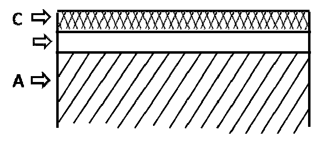
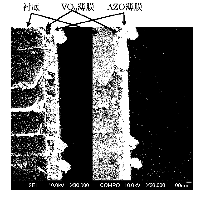
[0046] A quartz substrate deposited with a 100nm-thick vanadium dioxide film is placed in a sputtering chamber, vacuumed to less than 0.5 Pa, and an aluminum-doped oxide with a weight percentage of 99.5% aluminum: zinc molar ratio of 2:98 The zinc material is used as the target material, and high-purity argon is used as the working atmosphere. Argon is injected into the sputtering chamber at a flow rate of 10 sccm and the air pressure is kept below 1.0 Pa. The sputtering power is set at 180W, and the sputtering is performed for 20 minutes to obtain (AZO ) A composite thin film based on vanadium dioxide thin film, wherein the thickness of the transparent conductive film is 400nm.
Embodiment 2
[0048] (ATO) composite films based on vanadium dioxide films can also be prepared by a similar method: a quartz substrate deposited with a 20nm thick vanadium dioxide film is placed in a sputtering chamber, and the vacuum is lower than 4.0 Pa, and the content in weight percent 99%, antimony: tin molar ratio of 7:93 antimony-doped tin dioxide material is used as the target material, the working atmosphere adopts high-purity argon gas, and the argon gas is injected into the sputtering chamber at a flow rate of 40 sccm and the pressure is kept below 8.0 Pa, the sputtering power was set at 30W, and the sputtering time was 120 minutes to obtain a composite film based on (ATO) vanadium dioxide film, in which the thickness of the transparent conductive film was 340nm.
PUM
| Property | Measurement | Unit |
|---|---|---|
| Thickness | aaaaa | aaaaa |
| Thickness | aaaaa | aaaaa |
Abstract
Description
Claims
Application Information


