Nanoparticle films for use as solar cell back reflectors and other applications

a solar cell and back reflector technology, applied in the field of nanotechnology, can solve the problems of inability to meet the product reliability criteria, thin film si solar cells traditionally have lower efficiencies than wafer-based si counterparts, and the si layer may not be able to sufficiently absorb sunlight, and achieve the effect of low emissivity glass

Inactive Publication Date: 2014-10-23
THE SOUTH DAKOTA BOARD OF REGENTS
View PDF15 Cites 40 Cited by
  • Summary
  • Abstract
  • Description
  • Claims
  • Application Information

AI Technical Summary

Benefits of technology

[0034]In one aspect, the method further includes curing the nanoparticle film by IJV or thermal radiation. In a related aspect, the nanoparticle film is applied to a glass substrate, thereby resulting in low emissivity glass.

Problems solved by technology

However, thin film Si solar cells traditionally have lower efficiencies than their wafer-based Si counterparts, which is partially due to inadequate light absorption by the thin Si layer.
On the other hand, the Si layer may not be able to sufficiently absorb sunlight once it becomes too thin.
Despite its excellent reflectance, Ag film is not used in thin film Si products, as it is not able to meet the product reliability criteria for three main reasons in addition to cost: (1) Ag has a high mobility.
Once Ag reaches the Si absorber layer, it deteriorates the solar cell performance.
The problem starts most commonly from the edge of Ag film and advances laterally to the whole coating layer even though it is covered by a ZnO layer.
As solar panels require a long lifetime (>15 years), the conventionally processed Ag thin film back reflectors are not able to pass standard reliability tests, such as IEC 61215 and 61646.
In fact, the oxidation issue of Ag films has been a long-standing problem in low-emission glass coatings for buildings windows and in flat panel display devices.
(3) Ag thin films usually exhibit poor adhesion to most substrate materials, like stainless steel, plastic, and glass.
This eventually leads to device failure.
Further, metal based back reflector and buffer layer are deposited by high-vacuum sputtering process, which is time consuming, energy intensive, and has high material cost and waste.
Thin film photovoltaic technologies also face major challenges due to the scarcity of key elements.
Light trapping can be accomplished with conventional sputtered metal based back reflectors by depositing absorber on textured surface or by anisotropic etching of the absorber surface, but deposition of high quality absorber films with large grain size is challenging on rough surfaces and etching of absorber can deteriorate performance and is costly since absorber thickness is significantly reduced and can require lithography.
However, these pigmented back reflectors have only been applied to superstrate configured thin film solar cells; that is, the absorber material is deposited onto glass and the back reflector is the last layer deposited.
Organic materials and components, such as binders in white paint or encapsulate materials, are not suitable for a harsh processing environment as they can decompose, degas or otherwise contaminate the absorber materials and soil the deposition equipment.
Further, previously used methods, such as drop-casting, are very slow at obtaining thick pigmented diffuse back reflectors and not suitable for low cost, high speed manufacturing.

Method used


Image

  • Nanoparticle films for use as solar cell back reflectors and other applications
  • Nanoparticle films for use as solar cell back reflectors and other applications
  • Nanoparticle films for use as solar cell back reflectors and other applications

Examples


example 1

BaTiO3 Nanoparticle Films

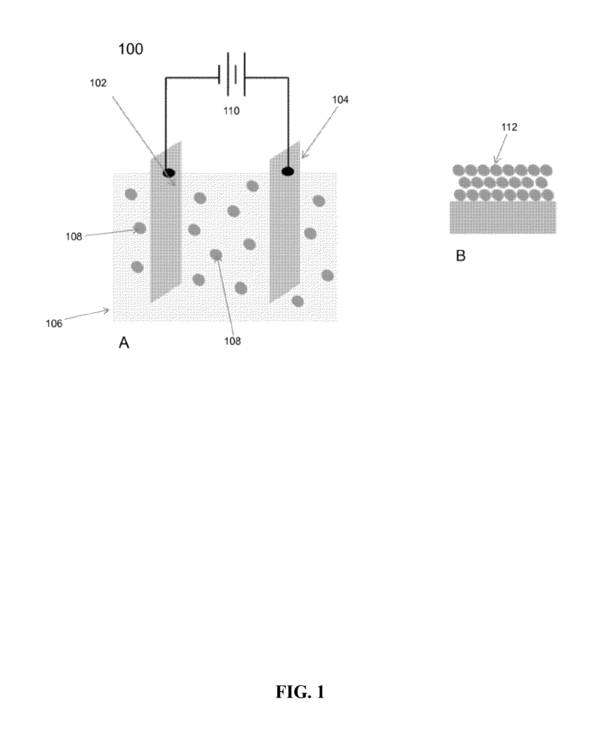
[0181]BaTiO3 nanoparticles were deposited onto either ITO coated glass substrates, silicon wafer (doped and undoped) substrates, or aluminum substrates using the apparatus shown in FIG. 1. Solutions comprising BaTiO3 nanoparticles (average diameter ˜700 nm) were prepared by adding 7.5 g BaTiO: nanoparticles to 150 mL of Blend A. Prior to electrophoretic deposition, the solutions were sonicated for about 5 to 30 min. Films of BaTiO3 nanoparticles were deposited onto the various substrates via electrophoretic deposition under the following conditions: a direct voltage of 60 V; a distance of 2 to 4 cm between the electrode (either Pt foil, ITO coated glass, or aluminum) and substrate; deposition times of 5 min; and deposition temperature of room temperature. Finally, the nanoparticle films were evaluated using standard techniques. The nanoparticle films were about 20 μm thick and exhibited a surface roughness in the range of from about 100 nm to about 3 μm. The...

example 2

Ag Nanoparticle Films

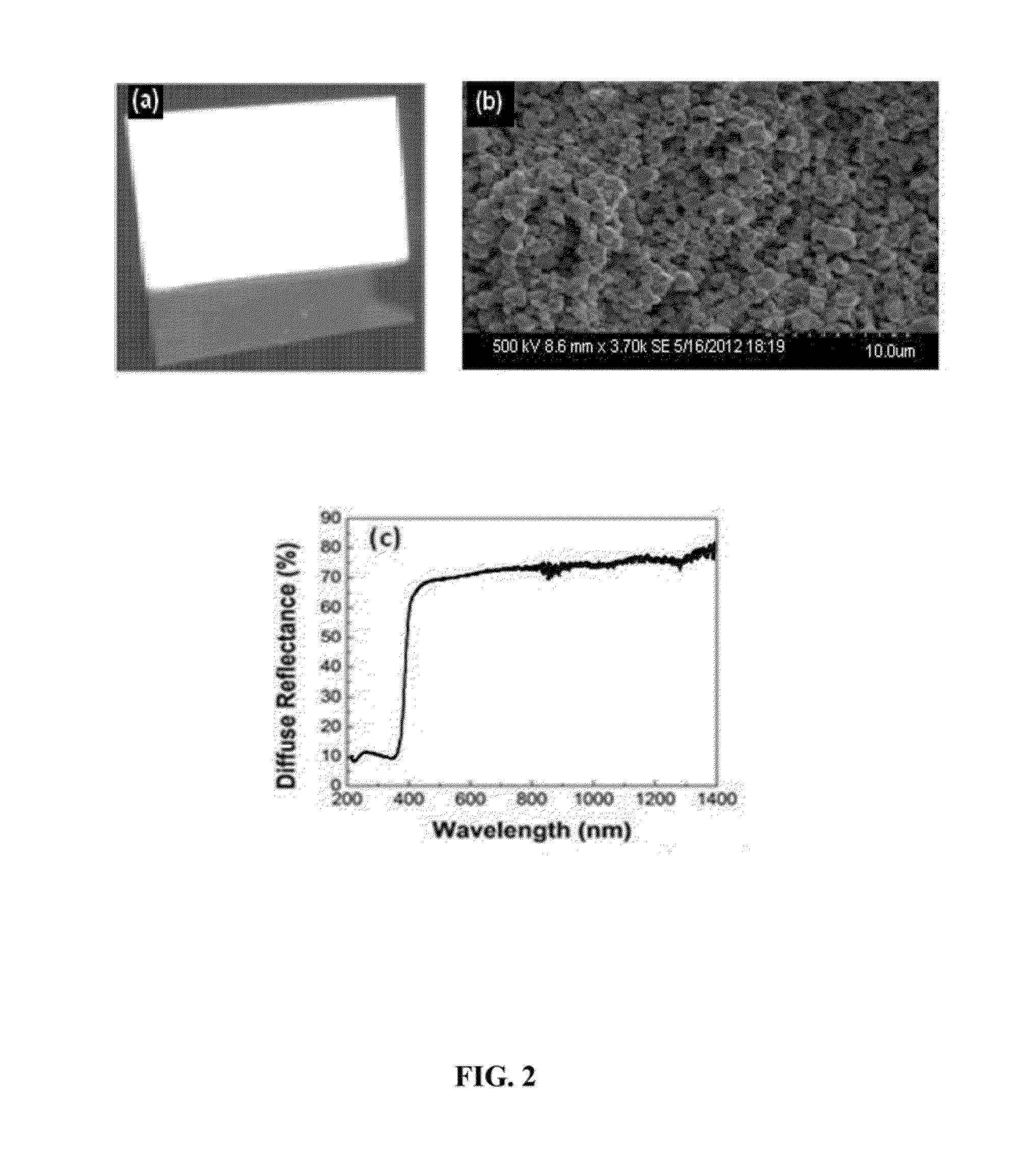
[0182]Ag nanoparticles were deposited onto ITO coated glass substrates using the apparatus shown in FIG. 1. Solutions comprising Ag nanoparticles (average diameter ˜50-80 nm) were prepared by adding 0.1 g Ag nanoparticles to 100 mL of Blend A. Prior to electrophoretic deposition, the solutions were sonicated for about 20 min. Films of Ag nanoparticles were deposited onto the substrates via electrophoretic deposition under the following conditions: a direct voltage of 60 V; a distance of 2 to 4 cm between the electrode (Pt foil) and substrate; and deposition times of 1 to 5 min. The normalized diffuse reflectance and transmission spectra of the film shown in FIG. 5 revealed that the film transmits visible wavelengths of light and reflects both UV and infrared wavelengths of light. These experimental results confirm that the deposited nanoparticle film is suitable for use as a low emissivity coating for a glass window.

example 3

Si Nanoparticle Films

[0183]Si nanoparticles were deposited onto ITO coated glass substrates using the apparatus shown in FIG. 1. Solutions comprising Si nanoparticles (American Elements, average diameter ˜130 nm) were prepared by adding 0.1 g Si nanoparticles to 40) mL of Blend A. Prior to electrophoretic deposition, the solutions were sonicated for about 20 min. Films of Si nanoparticles were deposited onto the substrates via electrophoretic deposition under the following conditions: a direct voltage of 5 to 60 V; a distance of 2 to 4 cm between the electrode (Pt foil or ITO coated glass) and substrate; and deposition times of 20 s to 6 min.


PUM

PropertyMeasurementUnit
diameteraaaaaaaaaa
diameteraaaaaaaaaa
thicknessaaaaaaaaaa

Abstract

Disclosed are methods for forming nanoparticle films using electrophoretic deposition. The methods comprise exposing a substrate to a solution, the solution comprising substantially dispersed nanoparticles, an organic solvent, and a polymer characterized by a backbone comprising Si—O groups. The methods further comprise applying an electric field to the solution, whereby a nanoparticle film is deposited on the substrate. Suitable polymers include polysiloxanes, polysilsesquioxanes and polysilicates. Coated glass windows and methods of forming the coated glass windows using the solutions are also disclosed. The methods may be adapted to form nanoparticle films suitable for use as back reflectors in solar cells, where such nanoparticle-based back reflectors exhibit high reflection and light scattering properties, including use of such back reflectors to fabricate solar cells and other photovoltaic-based and light dependent devices such as television screens, computer monitors, portable systems such as mobile phones, handheld games consoles and PDAs.

Description

CROSS REFERENCE TO RELATED APPLICATIONS[0001]This application claims benefit under 35 U.S.C. §119(e) to U.S. Provisional Application No. 61 / 752,033, filed Jan. 14, 2013, and 61 / 876,374, filed Sep. 11, 2013, each of which is incorporated by reference herein in their entireties.REFERENCE TO GOVERNMENT RIGHTS[0002]This invention was made with government support under 0903685 and 0903804 awarded by the National Science Foundation. The government has certain rights in the invention.BACKGROUND OF THE INVENTION[0003]1. Field of Invention[0004]The present invention relates generally to nanotechnology, and specifically to nanoparticle-film coating of substrates such as glass to provide low emissivity coatings and other surfaces to produce back reflectors, where the latter may be used in photovoltaic energy generation as a component for a solar cell that exhibits high reflection and light scattering properties.[0005]2. Background Information[0006]Emerging research in nanotechnology has led to...

Claims


Application Information

Patent Timeline
Patent Type & Authority Applications(United States)
IPC IPC(8): G02B5/02C25D7/08B29C67/20B05D3/02B05D1/00B05D1/02B05D1/30B05D1/28C25D13/02B05D1/18
CPCG02B5/0284Y10S977/892C25D7/08B29C67/20B05D1/18B05D1/005B05D1/02B05D1/305B05D1/28B05D3/0254Y10S977/834B82Y20/00Y10S977/774B82Y30/00B82Y40/00Y10S977/779C25D13/02H01L21/02422H01L21/02532H01L21/02554H01L21/02565H01L21/02601H01L21/02628H02S40/22H01L31/056Y02E10/52
Inventor BILLS, BRADENMORRIS, NATHANFAN, QI HUADUBEY, MUKULGALIPEAU, DAVID
Owner THE SOUTH DAKOTA BOARD OF REGENTS
Why Eureka
Try Eureka