Static protection structure

An electrostatic protection and electrostatic terminal technology, applied in the field of semiconductor electrostatic protection, can solve the problems of large magnification, high reverse breakdown voltage, low on-resistance, etc. The effect of current increase

Active Publication Date: 2015-12-02
SHANGHAI HUAHONG GRACE SEMICON MFG CORP
View PDF4 Cites 0 Cited by
  • Summary
  • Abstract
  • Description
  • Claims
  • Application Information

AI Technical Summary

Problems solved by technology

Generally, the reverse breakdown voltage of the high-voltage N-well / high-voltage P-well junction is relatively high, so the application of this structure is greatly limited
In addition, since the silicon-controlled rectifier itself is turned on, the parasitic NPN tube and the PNP tube realize the positive feedback of current amplification, resulting in a very low on-resistance and a large amplification factor, and the maintenance voltage after the snapback will be very low. Between 2 and 5V
The normal working voltage of high-voltage circuits is far above this, so using silicon controlled rectifiers as high-voltage electrostatic protection circuits is also prone to cause latch-up effects and is not easy to recover

Method used


Image

  • Static protection structure
  • Static protection structure
  • Static protection structure

Examples


Embodiment Construction

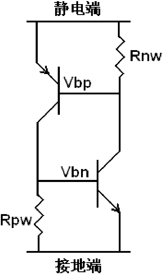
[0018] Electrostatic protection structure of the present invention, its equivalent circuit is as image 3 shown.

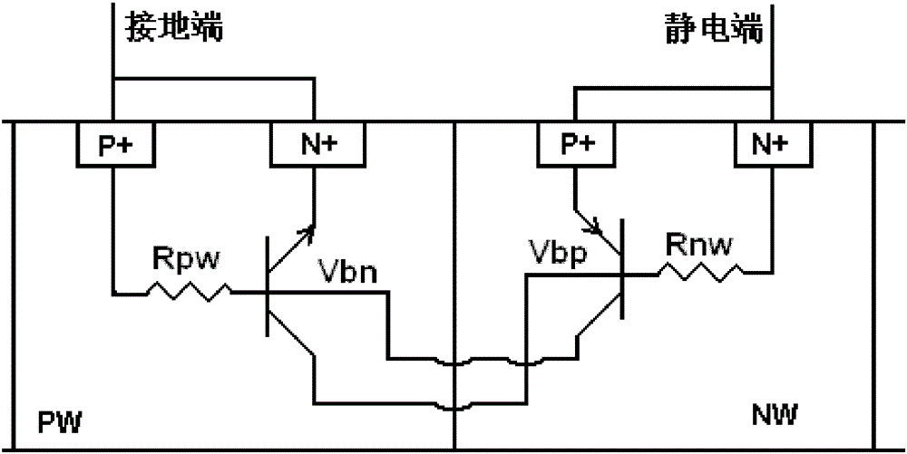
[0019] The electrostatic protection structure of the present invention comprises an N well and a P well, and these two wells are adjacent;

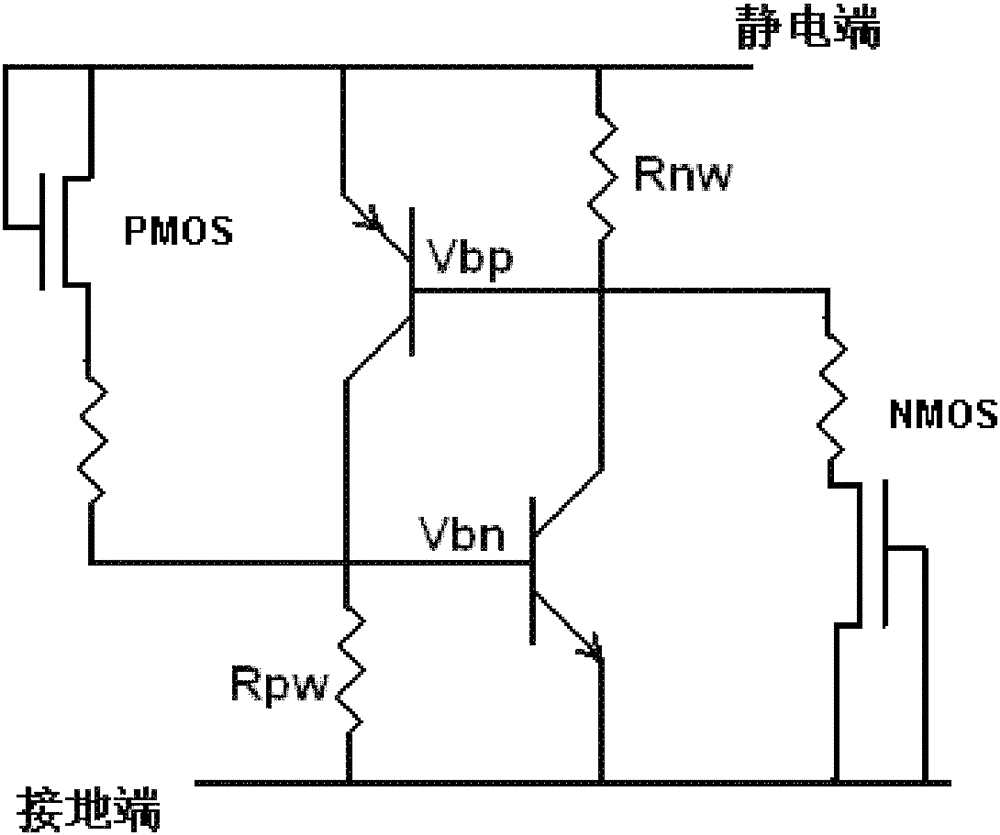
[0020] In the N well, a first P+ diffusion region, a second P+ diffusion region, a first N+ diffusion region, and a second N+ diffusion region are formed, and the first N+ diffusion region and the second N+ diffusion region are located in the first P+ diffusion region. region and the second P+ diffusion region, the first P+ diffusion region and the second P+ diffusion region constitute a PMOS transistor, and the first P+ diffusion region and the second P+ diffusion region are respectively used as the drain and source of the PMOS transistor. The gate of the PMOS transistor is formed above the channel region between the first P+ diffusion region and the second P+ diffusion region; one of the two P+ diffusion regions and one of...


PUM


Abstract

The invention discloses a static protective structure. The structure comprises an N trap and a P trap, wherein a first P+ diffusion zone, a second P+ diffusion zone, a first N+ diffusion zone and a second N+ diffusion zone are formed in the N trap; the first P+ diffusion zone and the second P+ diffusion zone form a PMOS (P-channel metal oxide semiconductor) tube; one of the two P+ diffusion zones and one of the two N+ diffusion zones in the N+ trap are in short connection with the grid electrode of the PMOS tube for connecting a static end; a third P+ diffusion zone, a fourth P+ diffusion zone, a third N+ diffusion zone and a fourth N+ diffusion zone are formed in the P trap, and an NMOS (N-channel metal oxide semiconductor) tube is formed by the third N+ diffusion zone and the fourth N+ diffusion zone; one of the two N+ diffusion zones and one of the two P+ diffusion zone in the P trap are in short circuit with the NMOS tube for connecting a ground end; the other N+ diffusion zone in the N trap and the other N+ diffusion zone in the P trap are in short connection; and the other P+ diffusion zone in the N trap and the other P+ diffusion zone in the P trap are in short connection. According to the static protective structure, the trigger voltage of electrostatic protection can be regulated conveniently and effectively, the latch effect can be effectively avoided, and the static discharge capability is strong.

Description

technical field [0001] The invention relates to semiconductor electrostatic protection technology, in particular to an electrostatic protection structure. Background technique [0002] As an electrostatic protection structure, the parasitic triode in the silicon-controlled rectifier (SCR) has a stronger electrostatic discharge capability than the metal-oxide-semiconductor field effect transistor (MOSFET). Generally, the electrostatic discharge capability of the silicon-controlled rectifier is 5 times that of the MOSFET. ~7 times. figure 1 Shown is a schematic cross-sectional structure diagram of an existing high trigger voltage silicon controlled rectifier. exist figure 1 Among them, the collector of the parasitic PNP transistor Vbp formed by P+ / high voltage N well / high voltage P well is also the base of the parasitic NPN transistor Vbn formed by N+ / high voltage P well / high voltage N well; similarly, N+ / high voltage P well / high voltage The collector of the parasitic NPN t...

Claims


Application Information

Patent Timeline
Patent Type & Authority Patents(China)
IPC IPC(8): H01L27/02H02H9/00
Inventor 苏庆
Owner SHANGHAI HUAHONG GRACE SEMICON MFG CORP
Why Eureka
Try Eureka