Electrode structure with grid lines on front surface

A technology of electrode structure and front grid line, which is applied in the direction of circuits, electrical components, semiconductor devices, etc., can solve the problem that the amount of paste used has not been reduced as expected, the efficiency of the battery has not been further improved, and the main grid line is easy to print offset etc. to achieve the effects of improving photoelectric conversion efficiency, reducing slurry, and reducing area

Active Publication Date: 2012-11-14
NINGBO ULICA SOLAR SCIENCE & TECHNOLOGY CO LTD
View PDF5 Cites 9 Cited by
  • Summary
  • Abstract
  • Description
  • Claims
  • Application Information

AI Technical Summary

Problems solved by technology

[0003] The website of the State Intellectual Property Office discloses a patent application document for a secondary overprinting process, which separates and prints the main grid line and the sub grid line of the front electrode by adding a printing process, but the patent application document only provides a process , simply printed the main grid lines and auxiliary grid lines separately, without redesigning the front grid line electrode structure, the cell efficiency was not further improved, and the amount of paste used did not get the expected reduction. The other two There is an alignment process in printing, and the busbars are easy to print offset, which makes it difficult to solder components

Method used


Image

  • Electrode structure with grid lines on front surface
  • Electrode structure with grid lines on front surface
  • Electrode structure with grid lines on front surface

Examples


Embodiment 1

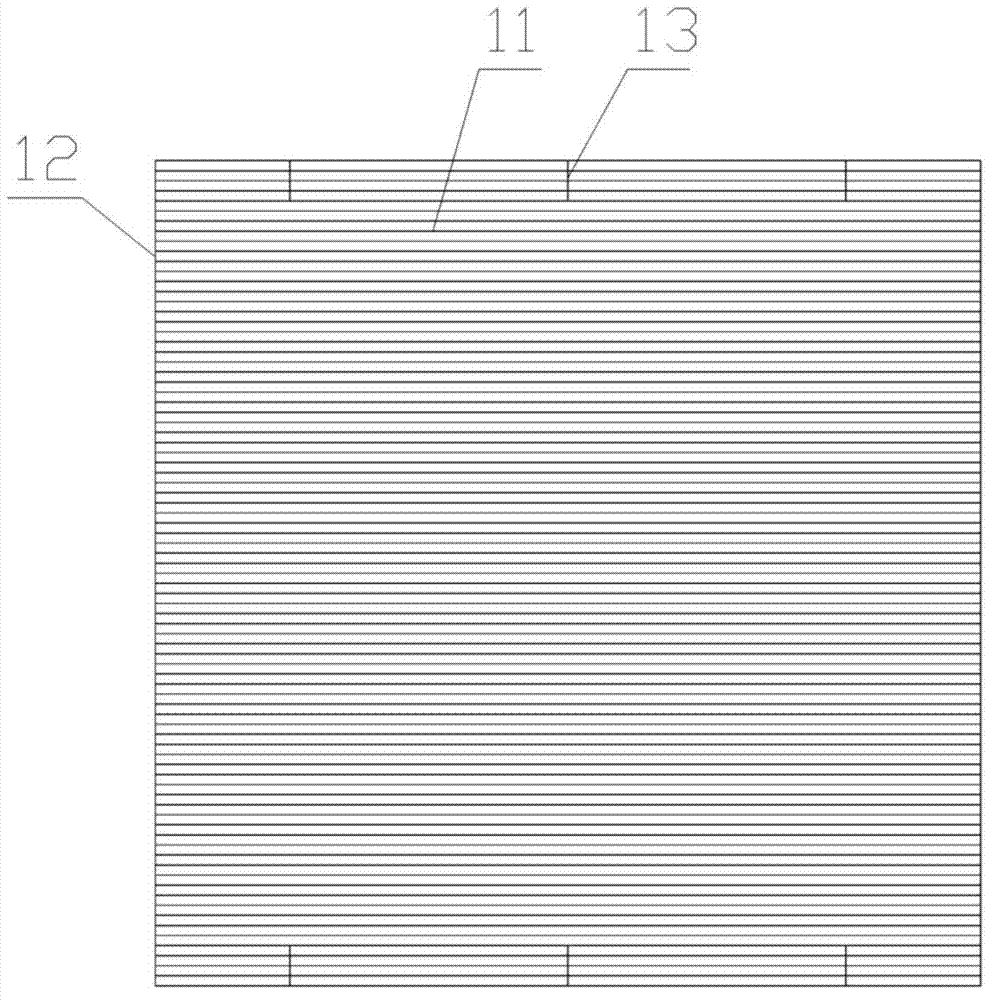
[0042] refer to Figure 1 to Figure 3 . The size of the polysilicon wafer is 156mm×156mm, Φ220mm. There are 3 main grid lines 20, the first sub-gate lines 11 and the second sub-gate lines 12 have a width of 50 μm, the third sub-gate lines 13 are 6, and the width is 180 μm, and the third sub-gate lines 13 are embedded The length of the portion 13b is 2 mm.

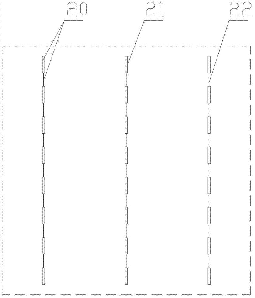
[0043] Each busbar 20 is composed of 8 rectangular sections 21 and 7 connecting lines 22 , the rectangular section 21 has a width of 1.6 mm and a length of 10.5 mm, and the connecting lines 22 have a length of 8.5 mm and a width of 150 μm.

[0044] After the above structural design of the front grid line electrode structure of the polysilicon wafer, the silver paste of the 20 parts of the main grid line can be saved by 42%, and the light-receiving area is also increased at the same time.

[0045] After the first and second printing of the polysilicon wafer that has undergone texturing, diffusion, etching and coating, it ...

Embodiment 2

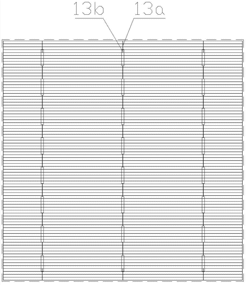
[0047] refer to Figure 4 to Figure 6 . The size of single crystal silicon wafer is 125mm×125mm, Φ165mm. There are two main gate lines 20, the first sub-gate lines 11 and the second sub-gate lines 12 have a width of 50 μm, the third sub-gate lines 13 are four, and the width is 220 μm, and the third sub-gate lines 13 are embedded The length of segment 13b is 1.5 mm.

[0048] Each busbar 20 is composed of 6 rectangular sections 21 and 5 connecting lines 22. The rectangular section 21 has a width of 1.6 mm and a length of 11 mm, and the connecting line 22 has a length of 9 mm and a width of 150 μm.

[0049] After the above structural design of the front grid line electrode structure of the polysilicon wafer, the silver paste of the 20 parts of the main grid line is saved by 43.2%, and the light receiving area is also increased.

[0050] After the polysilicon wafers that have been textured, diffused, etched, and coated have undergone the first and second printings, they are mou...


PUM


Abstract

The invention discloses an electrode structure with grid lines on the front surface. The electrode structure comprises a plurality of first secondary grid lines (11) and at least two main grid lines (20) which are intersected with the first secondary grid lines (11), wherein each main grid line (20) is divided into a plurality of sections which are connected through connecting lines (22); third secondary grid lines (13) are also arranged on the front section and the tail section of each main grid lines (20); internally embedded sections (13b) of each third secondary grid line (13) are overlapped with the corresponding front sections or tail sections; and exposed sections (13a) of each third secondary grid line (13) are intersected with the first secondary grid lines (11). By adopting the electrode structure with the grid lines on the front surface, in a secondary overprinting process, counterpoint printing can be quickly and accurately performed, the using amount of silver slurry is reduced, and the battery conversion efficiency is improved.

Description

technical field [0001] The invention relates to the technical field of crystalline silicon solar cells, in particular to a front grid line electrode structure of a crystalline silicon solar cell manufactured by a secondary overprinting process. Background technique [0002] In the front grid electrode of the solar cell, the function of the auxiliary grid is to collect photo-generated carriers. In order to reduce the series resistance, the larger the aspect ratio, the better, while the main grid is mainly for component welding, not to collect The function of the current, without pursuing the aspect ratio. But at present, since the main grid lines and the sub grid lines are printed with the same screen, while pursuing the aspect ratio of the sub grid lines, the height of the main grid lines will also increase accordingly, which increases the amount of silver paste used. Increased production costs. [0003] The website of the State Intellectual Property Office discloses a pat...

Claims


Application Information

Patent Timeline
Patent Type & Authority Applications(China)
IPC IPC(8): H01L31/0224
Inventor 刘伟陈筑詹国平刘晓巍蔡二辉徐晓群
Owner NINGBO ULICA SOLAR SCIENCE & TECHNOLOGY CO LTD
Why Eureka
Try Eureka