Silicon-based triple-junction solar battery using germanium as tunneling junction
A technology of solar cells and tunnel junctions, applied in the field of solar cells, can solve the problems of lattice mismatch and anti-phase domains of Si bottom cells, and achieve the effect of solving lattice mismatch, thin thickness, and reduced dislocation density
- Summary
- Abstract
- Description
- Claims
- Application Information
AI Technical Summary
Problems solved by technology
Method used
Image
Examples
Embodiment Construction
[0021] The present invention will be further described below in conjunction with drawings and embodiments.
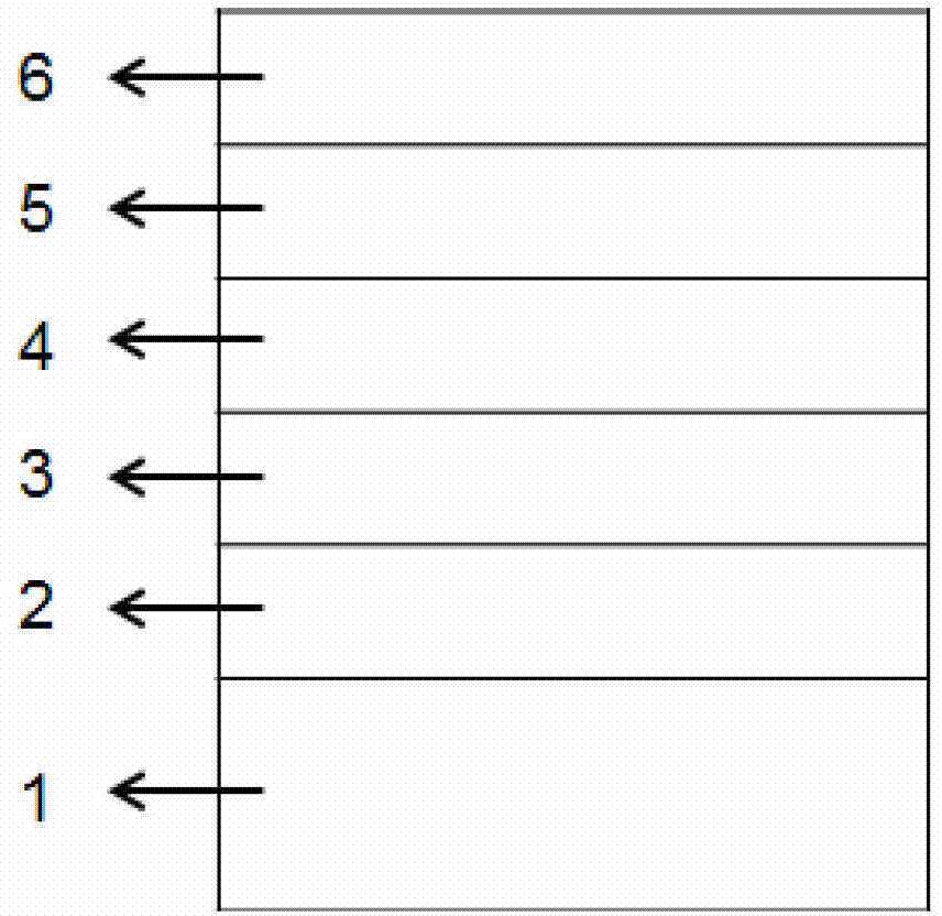
[0022] see figure 1 , the embodiment of the present invention is provided with a Si bottom cell 1, a Ge tunnel junction 2, a GaAs middle cell 3, an AlGaAs / InGaP tunnel junction 4, an InGaP top cell 5 and a contact layer 6, and the Si bottom cell 1 is constructed on a P-type On the Si substrate, the Ge tunneling junction 2 connects the Si bottom cell 1 and the GaAs middle cell 3 , the AlGaAs / InGaP tunneling junction 4 connects the GaAs middle cell 3 and the InGaP top cell 5 , and the contact layer 6 is provided on the InGaP top cell 5 .
[0023] The thickness of the P-type Si substrate may be 100-600 μm; the thickness of the Si substrate may be 100-600 μm, and the doping concentration may be 1×10 15 ~5×10 17 cm -3 .
[0024] The thickness of the emitter region of the Si bottom cell 1 may be 0.05-1 μm, and the doping concentration may be 1×10 18 ~5×10 19 cm -3 .
...
PUM
 Abstract
Description
Claims
Application Information
