Method for preparing zirconium nitride film on silicon substrate by magnetron sputtering

A technology of magnetron sputtering and radio frequency magnetron sputtering, applied in chemical instruments and methods, from chemically reactive gases, single crystal growth, etc., can solve the problem of large surface fluctuations, slow growth of ALD materials, and high-quality single crystals Issues such as the report of film growth results, to achieve the effects of small surface fluctuations, good application and promotion value, growth rate and film formation area

Active Publication Date: 2021-05-04
INST OF SEMICONDUCTORS - CHINESE ACAD OF SCI +1
View PDF8 Cites 1 Cited by
  • Summary
  • Abstract
  • Description
  • Claims
  • Application Information

AI Technical Summary

Problems solved by technology

Among them, the growth rate of ALD materials is slow. Although high-purity ZrN films with nanoscale thickness can be prepared, due to the low growth temperature, only amorphous or polycrystalline materials with poor crystal quality can be grown.
However, the preparation and growth of ZrN thin films by MOCVD is still in research and development, and there is no high-quality monolith that can achieve the X-ray rocking curve (XRC) half-maximum width (FWHM) of the ZrN (111) diffraction peak on Si substrates below 1°. Crystal thin film growth results report
The Institute of Semiconductors of the Chinese Academy of Sciences has used the ion beam epitaxy (IBE) process to grow ZrN thin films with a single preferred orientation. However, due to the small film area (2cm×2cm) of the ion beam epitaxy process, it is not suitable for the production of existing semiconductor devices. device
Magnetron sputtering is still the main process for preparing and growing ZrN thin films, but most of the existing research results are not conducive to the formation of ZrN due to the incomplete removal of the residual oxide layer on the surface of the Si substrate or the avoidance of the nitriding of the Si substrate surface first. Nucleated and grown amorphous Si x N y layer, or due to the relatively low heating temperature of the substrate or the relatively high sputtering power, most of the ZrN thin films have not grown on the Si substrate with a single preferred orientation and high crystal quality, and most research results have only obtained ZrN polycrystalline thin films with disordered orientation, and Surface relief is also large (AFM surface roughness (RMS) higher than 3nm)

Method used


Image

  • Method for preparing zirconium nitride film on silicon substrate by magnetron sputtering
  • Method for preparing zirconium nitride film on silicon substrate by magnetron sputtering
  • Method for preparing zirconium nitride film on silicon substrate by magnetron sputtering

Examples


Embodiment Construction

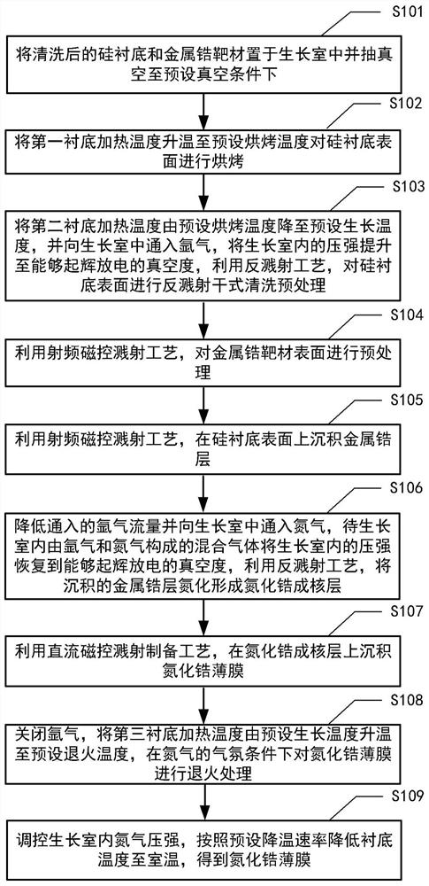
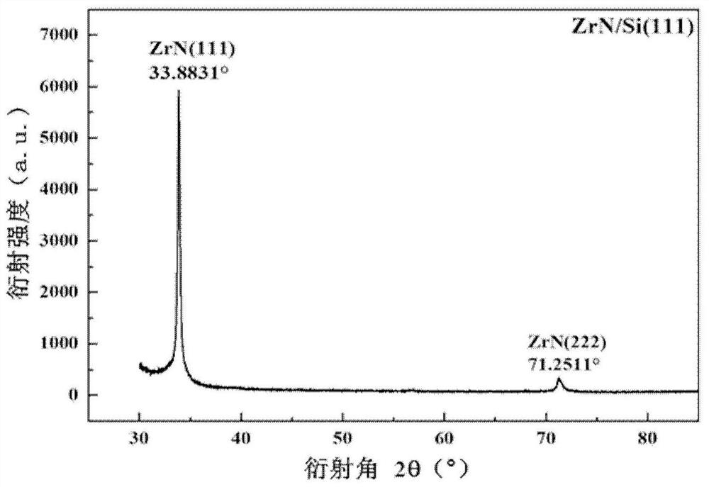
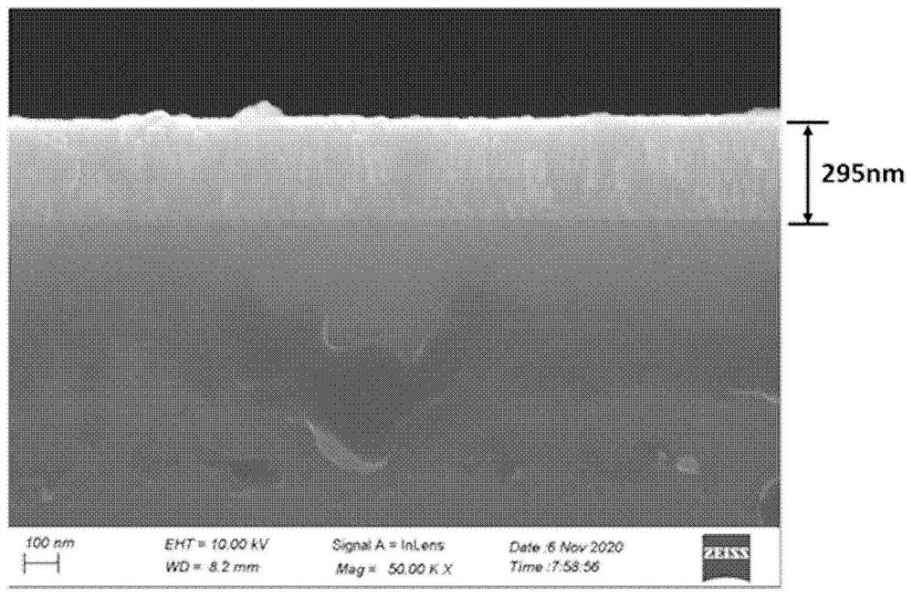
[0022] At present, due to the slow growth rate of silicon nitride deposition prepared by atomic layer deposition, although high-purity ZrN films with nanometer-scale thickness can be prepared, due to the low growth temperature, only amorphous or polycrystalline materials with poor crystalline quality can be grown; MOCVD process The preparation and growth of ZrN thin films is still in research and development, and there is no high-quality single crystal thin film that can realize the X-ray rocking curve (XRC) half-maximum width (FWHM) of the ZrN (111) diffraction peak on Si substrates below 1° The growth results are reported; the ion beam epitaxy (IBE) process realizes the growth of ZrN thin film with a single preferred orientation, but because of the small film area (2cm×2cm) of the ion beam epitaxy process, it is not suitable for making devices by using the existing semiconductor device process.

[0023] Magnetron sputtering is still the main process for preparing and growing ...


PUM

PropertyMeasurementUnit
sizeaaaaaaaaaa
surface roughnessaaaaaaaaaa

Abstract

The invention provides a method for preparing a zirconium nitride film on a silicon substrate by magnetron sputtering. The method comprises the following steps: placing the cleaned silicon substrate and a metal zirconium target material in a growth chamber under a preset vacuum condition; carrying out baking and reverse sputtering dry cleaning pretreatment on the surface of the silicon substrate at a preset temperature; carrying out radio frequency magnetron sputtering pretreatment on the surface of the metal zirconium target material; depositing a metal zirconium layer on the surface of the silicon substrate by using a radio frequency magnetron sputtering process; reducing the argon flow, introducing nitrogen into the growth chamber, and nitriding the deposited metal zirconium layer by using a reverse sputtering process to form a zirconium nitride nucleating layer; depositing a zirconium nitride film on the zirconium nitride nucleating layer by using a direct-current magnetron sputtering process; closing the argon, raising the heating temperature of the substrate to a preset annealing temperature, and annealing the zirconium nitride film under the nitrogen atmosphere condition; and regulating and controlling the nitrogen pressure in the growth chamber, and reducing the heating temperature of the substrate to room temperature according to a preset cooling rate to obtain the zirconium nitride film.

Description

technical field [0001] The invention belongs to the technical field of semiconductor and film material preparation, in particular to a method for preparing a zirconium nitride film on a silicon substrate by magnetron sputtering. Background technique [0002] Transition group refractory metal nitrides (including: titanium nitride (TiN), zirconium nitride (ZrN), hafnium nitride (HfN)) usually have a cubic rock-salt structure, which not only has good thermal and chemical stability, but also has good The electrical conductivity and resistivity are even comparable to some metal materials with good electrical conductivity. In the field of semiconductor technology, especially silicon-based device technology, transition group refractory metal nitride thin film materials have extremely important application value. For example, the magnetron sputtering and atomic layer deposition preparation processes of TiN films are relatively mature, and are the most commonly used interdiffusion b...

Claims


Application Information

Patent Timeline
Patent Type & Authority Applications(China)
IPC IPC(8): C30B25/06C30B25/10C30B25/16C30B25/18C30B29/38
CPCC30B25/06C30B25/183C30B25/186C30B25/16C30B29/38C30B25/10
Inventor 高洁杨少延魏洁魏鸿源陈怀浩
Owner INST OF SEMICONDUCTORS - CHINESE ACAD OF SCI
Why Eureka
Try Eureka