Novel dual-frequency patch antenna with resonance ring microstructure array

A micro-structure array, patch antenna technology, applied in the direction of antenna, antenna array, radiating element structure, etc., can solve the problems of pattern distortion, unfavorable mass production and processing, cross-polarization deterioration, etc., to avoid the size of the antenna. Increase, excellent radiation characteristics, solve the effect of easy distortion

Inactive Publication Date: 2012-11-14
UNIV OF ELECTRONICS SCI & TECH OF CHINA
View PDF8 Cites 6 Cited by
  • Summary
  • Abstract
  • Description
  • Claims
  • Application Information

AI Technical Summary

Problems solved by technology

[0004] (1) Passive component loading often destroys the excellent radiation characteristics of the original patch antenna, resulting in a decrease in the overall performance of the antenna, such as a decrease in radiation efficiency, pattern distortion, cross-polarization deterioration, etc.; at the same time, traditional passive component loading technology It will inevitably involve additional processing techniques such as vias, welding, and embedding, which makes the processing procedures very complicated, which is not conducive to large-scale production and processing.
[0005] (2) In order to ensure the performance of single-layer double-patch and double-layer double-patch, the lateral or cross-sectional size of the antenna is often increased, making the overall size of the antenna larger, so that this kind of antenna is difficult to meet the needs of antenna miniaturization in today's society
[0006] To sum up, the current dual-band antennas are difficult to achieve a balance between size and performance, and it is difficult to meet the actual needs of the market

Method used


Image

  • Novel dual-frequency patch antenna with resonance ring microstructure array
  • Novel dual-frequency patch antenna with resonance ring microstructure array
  • Novel dual-frequency patch antenna with resonance ring microstructure array

Examples


Embodiment 1

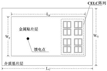
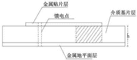
[0039] Such as figure 1 A top view of a double-sided copper-clad PCB is shown, and figure 2 The front view of the double-sided copper-clad PCB board is shown, in which the metal patch layer is located at the top and its area is smaller than the dielectric substrate layer. The number of the metal patch layer is one layer and it is made of copper; the dielectric substrate layer is located on the Below the metal patch layer, its length, width and height are:

[0040] W G =λ / 1.2

[0041] L G =λ / 1.7

[0042] h=λ / 170

[0043] Wherein λ is the vacuum wavelength corresponding to the central operating frequency of the low frequency band of the patch antenna; a metal ground plane layer is also fixed below the dielectric substrate layer, and the length and width of the metal ground plane layer are the same as the dielectric substrate layer, wherein There is also a feed point installed on the metal patch layer, and the feed point is a linear distance from the left side of the metal...

Embodiment 2

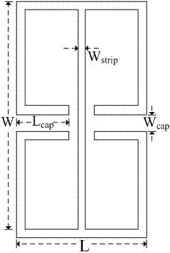
[0061] Such as Figure 9 The difference between the top view of the patch antenna shown in Embodiment 1 is that the radiating unit adopts the following Figure 8 The CSRR single-ring unit shown, the CSRR single-ring unit is a square surrounded by four grooves, one side is broken from the middle to form two fractures, and the two fractures are bent 90 degrees to the inside of the square After that, extend a small section parallel to each other, such as 1cm. The distance between two of the fractures:

[0062] W cap =λ / 1713

[0063] The length of the fracture is:

[0064] L cap =λ / 144.3.

[0065] The resonant ring microstructure array is formed by arranging a total of 3 x 3 CSRR single-ring units etched on the metal patch layer.

[0066] Since the entire array has 9 CSRR single-ring units, the area where the dielectric constant of the dielectric substrate can be affected by CSRR is larger than that of the CELC in Example 1, which can further increase the high-to-low freque...

Embodiment 3

[0069] The difference from Embodiment 1 is that in this embodiment, the resonant ring microstructure array consists of Figure 11 The four CSRR bicyclic units shown are arranged in an arrangement.

[0070] Such as Figure 10 The CSRR double-ring unit shown has two inner rectangles surrounded by bar-shaped grooves

[0071] and the outer rectangle. The inner rectangle is located inside the outer rectangle, and there is an opening in the middle of one long side of the outer rectangle. The width of the opening is: W cap =λ / 1754; At the same time, an opening is also provided in the middle of a side that is parallel to the long side of the outer rectangle and away from the long side of the inner rectangle, and the length of the opening is also W cap .

[0072] The remaining implementation methods are the same as those in Embodiment 1.


PUM


Abstract

The invention discloses a novel dual-frequency patch antenna with a resonance ring microstructure array, and belongs to the field of communication engineering. The novel dual-frequency patch antenna comprises a double-sided copper-clad PCB (printed circuit board) which is integrally formed by sequentially overlapping a metal patch layer, a medium substrate layer and a metal ground plane layer; one metal patch layer is provided, and a radiation array which is used for keeping a high radiation efficiency and an excellent radiation directional diagram at dual bands is etched on the surface of the metal patch layer. By the novel patch antenna, the defaults that, in the prior art, the dual-frequency patch antenna is large in size, or the radiation direction is easy to distort, the radiation intensity is reduced, and the cross polarization is deteriorated are overcome; the miniaturization is guaranteed, and high radiation efficiency and excellent radiation directional diagram are realized; and furthermore, the novel dual-frequency patch antenna does not need processing technologies such as passing through holes, welding and embedding, and the novel dual-frequency patch antenna is very suitable for mass manufacturing, processing and production.

Description

technical field [0001] The invention belongs to the technical field of antennas in communication engineering, and in particular relates to a novel dual-frequency patch antenna based on a resonant ring microstructure array. Background technique [0002] The dual-frequency system is a wireless communication system that can work simultaneously on two frequency bands, and is an important part of the existing wireless communication technology. At present, dual-band work is widely used in important occasions such as mobile phone communication, satellite communication, wireless local area network, and dual-band radar. Therefore, it is very important to design an antenna that can work in dual-band at the same time and has excellent performance. [0003] Patch antennas are popular for their low profile, small size, light weight, low cost, easy conformal design, and easy integration with active devices and circuits into a single module. In modern wireless communication systems, trad...

Claims


Application Information

Patent Timeline
Patent Type & Authority Applications(China)
IPC IPC(8): H01Q1/38H01Q5/01H01Q21/00H01Q5/10
Inventor 熊江林先其王秉中
Owner UNIV OF ELECTRONICS SCI & TECH OF CHINA
Why Eureka
Try Eureka